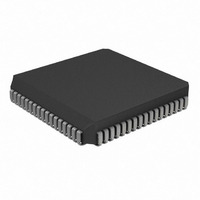
PIC17C756AT-33/L Microchip Technology, PIC17C756AT-33/L Datasheet - Page 62

PIC17C756AT-33/L
Manufacturer Part Number
PIC17C756AT-33/L
Description
IC MCU OTP 16KX16 A/D PWM 68PLCC
Manufacturer
Microchip Technology
Series
PIC® 17Cr
Datasheets
1.PIC16F616T-ISL.pdf
(8 pages)
2.PIC17C752-16L.pdf
(304 pages)
3.PIC17C752-16L.pdf
(6 pages)
Specifications of PIC17C756AT-33/L
Core Processor
PIC
Core Size
8-Bit
Speed
33MHz
Connectivity
I²C, SPI, UART/USART
Peripherals
Brown-out Detect/Reset, POR, PWM, WDT
Number Of I /o
50
Program Memory Size
32KB (16K x 16)
Program Memory Type
OTP
Ram Size
902 x 8
Voltage - Supply (vcc/vdd)
4.5 V ~ 5.5 V
Data Converters
A/D 12x10b
Oscillator Type
External
Operating Temperature
0°C ~ 70°C
Package / Case
68-PLCC
Processor Series
PIC17C
Core
PIC
Data Bus Width
8 bit
Data Ram Size
902 B
Interface Type
I2C, MSSP, RS- 232, SCI, SPI, USART
Maximum Clock Frequency
33 MHz
Number Of Programmable I/os
50
Number Of Timers
8
Operating Supply Voltage
3 V to 5.5 V
Maximum Operating Temperature
+ 70 C
Mounting Style
SMD/SMT
Minimum Operating Temperature
0 C
On-chip Adc
12 bit
For Use With
AC164308 - MODULE SKT FOR PM3 68PLCCDVA17XL681 - DEVICE ADAPTER FOR PIC17C752DM173001 - KIT DEVELOPMENT PICDEM17AC174007 - MODULE SKT PROMATEII 68PLCCAC164024 - ADAPTER PICSTART PLUS 68PLCC
Lead Free Status / RoHS Status
Lead free / RoHS Compliant
Eeprom Size
-
Lead Free Status / Rohs Status
Details
Available stocks
Company
Part Number
Manufacturer
Quantity
Price
Company:
Part Number:
PIC17C756AT-33/L
Manufacturer:
Microchip Technology
Quantity:
10 000
- Current page: 62 of 304
- Download datasheet (6Mb)
PIC17C7XX
8.2
Table writes to external memory are always two-cycle
instructions. The second cycle writes the data to the
external memory location. The sequence of events for
an external memory write are the same for an internal
write.
8.2.1
The “i” operand of the TABLWT instruction can specify
that the value in the 16-bit TBLPTR register is automat-
ically incremented (for the next write). In Example 8-1,
the TBLPTR register is not automatically incremented.
FIGURE 8-5:
DS30289B-page 62
Table Writes to External Memory
Note: If external write and GLINTD = ’1’ and Enable bit = ’1’, then when ’1’
TABLE WRITE CODE
The highest pending interrupt is cleared.
AD15:AD0
Instruction
Instruction
Executed
Fetched
TABLWT WRITE TIMING (EXTERNAL MEMORY)
ALE
WR
OE
OE
Q1 Q2 Q3 Q4
’1’
INST (PC-1)
TABLWT
PC
Q1 Q2 Q3 Q4
TABLWT cycle1
INST (PC+1)
PC+1
EXAMPLE 8-1:
CLRWDT
MOVLW
MOVWF
MOVLW
MOVWF
MOVLW
TLWT
MOVLW
TABLWT
Data write cycle
Q1 Q2 Q3 Q4
TABLWT cycle2
TBL
HIGH (TBL_ADDR) ; Load the Table
TBLPTRH
LOW (TBL_ADDR)
TBLPTRL
HIGH (DATA)
1, WREG
LOW (DATA)
0,0,WREG
Flag bit, do table write.
Data out
Q1 Q2 Q3 Q4
TABLE WRITE
INST (PC+2)
INST (PC+1)
2000 Microchip Technology Inc.
PC+2
;
; Clear WDT
;
;
;
; Load HI byte
;
; Load LO byte
;
;
;
program memory
address
in TABLATH
in TABLATL
and write to
(Ext. SRAM)
Related parts for PIC17C756AT-33/L
Image
Part Number
Description
Manufacturer
Datasheet
Request
R

Part Number:
Description:
IC MCU OTP 16KX16 A/D PWM 68PLCC
Manufacturer:
Microchip Technology
Datasheet:

Part Number:
Description:
IC MCU OTP 16KX16 A/D PWM 68PLCC
Manufacturer:
Microchip Technology
Datasheet:

Part Number:
Description:
IC MCU CMOS 33MHZ 16K EPRM68PLCC
Manufacturer:
Microchip Technology
Datasheet:

Part Number:
Description:
High-Performance 8-bit CMOS EPROM Microcontrollers with 10-bit A/D
Manufacturer:
MICROCHIP [Microchip Technology]
Datasheet:

Part Number:
Description:
IC MCU OTP 16KX16 A/D PWM 64TQFP
Manufacturer:
Microchip Technology
Datasheet:

Part Number:
Description:
IC MCU OTP 16KX16 A/D PWM 64TQFP
Manufacturer:
Microchip Technology
Datasheet:

Part Number:
Description:
IC MCU OTP 16KX16 A/D PWM 64TQFP
Manufacturer:
Microchip Technology
Datasheet:

Part Number:
Description:
IC MCU EPROM 16KX16 A/D 68CLCC
Manufacturer:
Microchip Technology
Datasheet:

Part Number:
Description:
IC MCU CMOS 16MHZ 16K EPRM68PLCC
Manufacturer:
Microchip Technology
Datasheet:

Part Number:
Description:
IC MCU CMOS 16MHZ 16K EPRM64TQFP
Manufacturer:
Microchip Technology
Datasheet:

Part Number:
Description:
IC MCU CMOS 33MHZ 16K EPRM64TQFP
Manufacturer:
Microchip Technology
Datasheet:

Part Number:
Description:
IC, 8BIT MCU, PIC17C, 33MHZ, PLCC-64
Manufacturer:
Microchip Technology
Datasheet:

Part Number:
Description:
IC,MICROCONTROLLER,8-BIT,PIC CPU,CMOS,QFP,64PIN,PLASTIC
Manufacturer:
Microchip Technology
Datasheet:

Part Number:
Description:
MICRO CTRL 16K MEMORY OTP 64SDIP
Manufacturer:
Microchip Technology
Datasheet:


