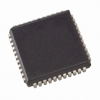
AT89C51AC3-SLSUM Atmel, AT89C51AC3-SLSUM Datasheet - Page 22

AT89C51AC3-SLSUM
Manufacturer Part Number
AT89C51AC3-SLSUM
Description
IC 8051 MCU FLASH 64K 44PLCC
Manufacturer
Atmel
Series
89Cr
Datasheet
1.AT89C51AC3-RLTUM.pdf
(140 pages)
Specifications of AT89C51AC3-SLSUM
Core Processor
8051
Core Size
8-Bit
Speed
60MHz
Connectivity
UART/USART
Peripherals
POR, PWM, WDT
Number Of I /o
36
Program Memory Size
64KB (64K x 8)
Program Memory Type
FLASH
Eeprom Size
2K x 8
Ram Size
2.25K x 8
Voltage - Supply (vcc/vdd)
3 V ~ 5.5 V
Data Converters
A/D 8x10b
Oscillator Type
External
Operating Temperature
-40°C ~ 85°C
Package / Case
44-PLCC
Processor Series
AT89x
Core
8051
Data Bus Width
8 bit
Data Ram Size
2304 B
Interface Type
UART, SPI
Maximum Clock Frequency
60 MHz
Number Of Programmable I/os
36
Number Of Timers
3
Operating Supply Voltage
3 V to 5.5 V
Maximum Operating Temperature
+ 85 C
Mounting Style
SMD/SMT
3rd Party Development Tools
PK51, CA51, A51, ULINK2
Minimum Operating Temperature
- 40 C
On-chip Adc
10 bit, 8 Channel
Package
44PLCC
Device Core
8051
Family Name
89C
Maximum Speed
60 MHz
For Use With
AT89OCD-01 - USB EMULATOR FOR AT8XC51 MCU
Lead Free Status / RoHS Status
Lead free / RoHS Compliant
Available stocks
Company
Part Number
Manufacturer
Quantity
Price
External Space
Memory Interface
External Bus Cycles
22
AT89C51AC3
The external memory interface comprises the external bus (port 0 and port 2) as well as
the bus control signals (RD#, WR#, and ALE).
Figure 10 shows the structure of the external address bus. P0 carries address A7:0
while P2 carries address A15:8. Data D7:0 is multiplexed with A7:0 on P0. Table 5
describes the external memory interface signals.
Figure 10. External Data Memory Interface Structure
Table 5. External Data Memory Interface Signals
This section describes the bus cycles the AT89C51AC3 executes to read (see
Figure 11), and write data (see Figure 12) in the external data memory.
External memory cycle takes 6 CPU clock periods. This is equivalent to 12 oscillator
clock period in standard mode or 6 oscillator clock periods in X2 mode. For further infor-
mation on X2 mode.
Slow peripherals can be accessed by stretching the read and write cycles. This is done
using the M0 bit in AUXR register. Setting this bit changes the width of the RD# and
WR# signals from 3 to 15 CPU clock periods.
For simplicity, the accompanying figures depict the bus cycle waveforms in idealized
form and do not provide precise timing information. For bus cycle timing parameters
refer to the Section “AC Characteristics” of the AT89C51AC3 datasheet.
Signal
Name
AD7:0
A15:8
WR#
RD#
ALE
Type
I/O
O
O
O
O
Description
Address Lines
Upper address lines for the external bus.
Address/Data Lines
Multiplexed lower address lines and data for the external
memory.
Address Latch Enable
ALE signals indicates that valid address information are available
on lines AD7:0.
Read
Read signal output to external data memory.
Write
Write signal output to external memory.
AT89C51AC3
WR#
RD#
ALE
P2
P0
AD7:0
A15:8
Latch
A7:0
A15:8
A7:0
D7:0
OE
WR
PERIPHERAL
RAM
4383D–8051–02/08
Alternative
Function
P2.7:0
P0.7:0
P3.7
P3.6
-


