PIC12C508A/JW Microchip Technology, PIC12C508A/JW Datasheet - Page 32
PIC12C508A/JW
Manufacturer Part Number
PIC12C508A/JW
Description
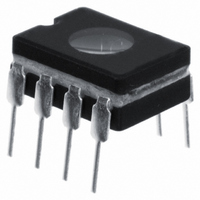
IC MCU EPROM 512X12 8CDIP
Manufacturer
Microchip Technology
Series
PIC® 12Cr
Datasheets
1.PIC12C508A-04SM.pdf
(113 pages)
2.PIC12C508A-04SM.pdf
(6 pages)
3.PIC12C508A-04SM.pdf
(16 pages)
4.PIC12C508A-04SM.pdf
(4 pages)
Specifications of PIC12C508A/JW
Core Processor
PIC
Core Size
8-Bit
Speed
4MHz
Peripherals
POR, WDT
Number Of I /o
5
Program Memory Size
768B (512 x 12)
Program Memory Type
EPROM, UV
Ram Size
25 x 8
Voltage - Supply (vcc/vdd)
3 V ~ 5.5 V
Oscillator Type
Internal
Operating Temperature
0°C ~ 70°C
Package / Case
8-CDIP (0.300", 7.62mm) Window
For Use With
ISPICR1 - ADAPTER IN-CIRCUIT PROGRAMMINGDVMCPA - KIT DVR BOARD EVAL SYSTEM MXDEV1DVA12XP080 - ADAPTER DEVICE FOR MPLAB-ICEAC124001 - MODULE SKT PROMATEII 8DIP/SOIC
Lead Free Status / RoHS Status
Contains lead / RoHS non-compliant
Eeprom Size
-
Data Converters
-
Connectivity
-
Available stocks
Company
Part Number
Manufacturer
Quantity
Price
Company:

Part Number:
PIC12C508A/JW
Manufacturer:
MICROCHIP
Quantity:
105


PIC12C5XX
FIGURE 7-3:
FIGURE 7-4:
7.2
After generating a START condition, the bus master
transmits a control byte consisting of a slave address
and a Read/Write bit that indicates what type of opera-
tion is to be performed. The slave address consists of
a 4-bit device code (1010) followed by three don’t care
bits.
The last bit of the control byte determines the operation
to be performed. When set to a one a read operation is
selected, and when set to a zero a write operation is
selected. (Figure 7-5). The bus is monitored for its cor-
responding slave address all the time. It generates an
acknowledge bit if the slave address was true and it is
not in a programming mode.
DS40139E-page 32
SCL
SDA
SCL
SDA
(A)
Device Addressing
CONDITION
START
(B)
DATA TRANSFER SEQUENCE ON THE SERIAL BUS
ACKNOWLEDGE TIMING
1
Transmitter must release the SDA line at this point
allowing the Receiver to pull the SDA line low to
acknowledge the previous eight bits of data.
2
3
Data from transmitter
4
ACKNOWLEDGE
ADDRESS OR
VALID
5
(C)
6
TO CHANGE
ALLOWED
7
DATA
Acknowledge
FIGURE 7-5:
8
Start Bit
Bit
S
9
1
Device Select
(D)
1
Receiver must release the SDA line at this point
so the Transmitter can continue sending data.
0
Bits
Data from transmitter
CONTROL BYTE FORMAT
Slave Address
1
2
0
1999 Microchip Technology Inc.
3
Read/Write Bit
Don’t Care
X
Acknowledge Bit
Bits
X
X
CONDITION
R/W
STOP
(C)
ACK
(A)
Related parts for PIC12C508A/JW
Image
Part Number
Description
Manufacturer
Datasheet
Request
R

Part Number:
Description:
8-Pin/ 8-Bit CMOS Microcontrollers
Manufacturer:
Microchip Technology
Part Number:
Description:
8-Pin/ 8-Bit CMOS Microcontroller with EEPROM Data Memory
Manufacturer:
Microchip Technology
Part Number:
Description:
IC, 8BIT MCU, PIC12, 32MHZ, DFN-8
Manufacturer:
Microchip Technology
Datasheet:
Part Number:
Description:
IC, 8BIT MCU, PIC12, 32MHZ, DFN-8
Manufacturer:
Microchip Technology
Datasheet:

Part Number:
Description:
Manufacturer:
Microchip Technology Inc.
Datasheet:
Part Number:
Description:
Manufacturer:
Microchip Technology Inc.
Datasheet:
Part Number:
Description:
Manufacturer:
Microchip Technology Inc.
Datasheet:
Part Number:
Description:
Manufacturer:
Microchip Technology Inc.
Datasheet:
Part Number:
Description:
Manufacturer:
Microchip Technology Inc.
Datasheet:
Part Number:
Description:
Manufacturer:
Microchip Technology Inc.
Datasheet:
Part Number:
Description:
Manufacturer:
Microchip Technology Inc.
Datasheet: