EP7309-CVZ Cirrus Logic Inc, EP7309-CVZ Datasheet - Page 31
EP7309-CVZ
Manufacturer Part Number
EP7309-CVZ
Description
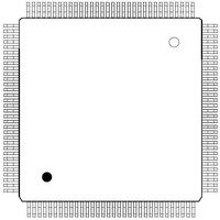
IC ARM720T MCU 74MHZ 208-LQFP
Manufacturer
Cirrus Logic Inc
Series
EP7r
Specifications of EP7309-CVZ
Core Size
32-Bit
Core Processor
ARM7
Speed
74MHz
Connectivity
Codec, DAI, EBI/EMI, IrDA, Keypad, SPI/Microwire1, UART/USART
Peripherals
LCD, LED, MaverickKey, POR, PWM
Number Of I /o
27
Program Memory Type
ROMless
Ram Size
56K x 8
Voltage - Supply (vcc/vdd)
2.3 V ~ 2.7 V
Oscillator Type
External
Operating Temperature
0°C ~ 70°C
Package / Case
208-LQFP
Controller Family/series
(ARM7)
No. Of I/o's
27
Ram Memory Size
48KB
Cpu Speed
74MHz
No. Of Timers
2
No. Of Pwm Channels
2
Digital Ic Case Style
LQFP
Embedded Interface Type
SSI, UART
Rohs Compliant
Yes
Processor Series
EP73xx
Core
ARM720T
Data Bus Width
32 bit
Mounting Style
SMD/SMT
3rd Party Development Tools
MDK-ARM, RL-ARM, ULINK2
Lead Free Status / RoHS Status
Lead free / RoHS Compliant
Eeprom Size
-
Program Memory Size
-
Data Converters
-
Lead Free Status / Rohs Status
Details
Other names
598-1214
Available stocks
Company
Part Number
Manufacturer
Quantity
Price


DS507F2
Ball Location
B10
B11
B12
B13
B14
B15
B16
C10
C11
C12
C13
C14
C15
C16
D10
D11
D12
D13
D14
D15
D16
B7
B8
B9
C1
C2
C3
C4
C5
C6
C7
C8
C9
D1
D2
D3
D4
D5
D6
D7
D8
D9
E1
E2
E3
E4
E5
E6
Table 20. 256-Ball PBGA Ball Listing (Continued)
VDDCORE
nEXTPWR
nURESET
WAKEUP
EXPRDY
EXPCLK
VSSRTC
nPWRFL
MOSCIN
VDDIO
VDDIO
VDDIO
VDDIO
VDDIO
WRITE
VDDIO
VDDIO
RXD[2]
WORD
VSSIO
VSSIO
VSSIO
VSSIO
VSSIO
VSSIO
VSSIO
VSSIO
VSSIO
VSSIO
nCS[2]
nMWE
VSSIO
VSSIO
nCS[0]
Name
nPOR
DD[2]
PB[7]
CL[1]
CL[2]
D[1]
A[2]
A[4]
A[5]
N/C
D[4]
D[7]
D[8]
TDI
Core ground Real time clock ground
Pad ground I/O ground
Pad ground I/O ground
Pad ground I/O ground
Pad ground I/O ground
Pad ground I/O ground
Core power Digital core power, 2.5V
Pad ground I/O ground
Pad ground I/O ground
Pad ground I/O ground
Pad ground I/O ground
Pad ground I/O ground
Pad ground I/O ground
Pad ground I/O ground
Pad power
Pad power
Pad power
Pad power
Pad power
Pad power
Pad power
Type
I/O
I/O
I/O
I/O
O
O
O
O
O
O
O
O
O
O
O
O
I
I
I
I
I
I
I
I
I
I
I
LCD serial display data
LCD line clock
Data I/O
System byte address
System byte address
System byte address
System wake up input
Digital I/O power, 3.3V
User reset input
Digital I/O power, 3.3V
Expansion clock input
Digital I/O power, 3.3V
Digital I/O power, 3.3V
Digital I/O power, 3.3V
Power-on reset input
External power supply sense input
Transfer direction
Expansion port ready input
Digital I/O power, 3.3V
Chip select out
ROM, expansion write enable
LCD pixel clock out
Data I/O
Power fail sense input
Main oscillator input
Digital I/O power, 3.3V
Data I/O
Data I/O
UART 2 receive data input
GPIO port B
JTAG data input
Word access select output
Chip select out
Description
Copyright Cirrus Logic, Inc. 2011
(All Rights Reserved)
Ball Location
G10
G12
G13
G14
G15
G16
E10
E11
E12
E13
E14
E15
E16
F10
F11
F12
F13
F14
F15
F16
G11
G1
G2
G3
G4
G5
G6
G7
G8
G9
H1
H2
H3
H4
H5
E7
E8
E9
F1
F2
F3
F4
F5
F6
F7
F8
F9
Table 20. 256-Ball PBGA Ball Listing (Continued)
nMEDCHG/nBROM
High-Performance, Low-Power System on Chip
PB[1]/PRDY[2]
RUN/CLKEN
nBATCHG
VSSOSC
VSSRTC
VSSRTC
VSSRTC
VSSRTC
BATOK
VSSIO
VDDIO
VSSIO
TXD[2]
VSSIO
VSSIO
VDDIO
VDDIO
VSSIO
VSSIO
Name
PB[5]
PB[3]
DD[3]
PB[4]
PB[6]
DD[0]
D[10]
D[11]
D[12]
D[13]
PA[7]
PA[5]
PA[4]
PA[6]
FRM
TDO
D[5]
D[9]
D[6]
D[3]
N/C
A[0]
N/C
A[1]
A[7]
A[8]
A[9]
Core ground Real time clock ground
RTC ground Real time clock ground
RTC ground Real time clock ground
RTC ground Real time clock ground
Pad ground I/O ground
Pad ground I/O ground
Pad ground I/O ground
Pad ground I/O ground
Pad ground I/O ground
Pad ground I/O ground
Pad power
Pad power
Pad power
Oscillator
ground
Type
I/O
I/O
I/O
I/O
I/O
I/O
I/O
I/O
O
O
O
O
O
O
O
O
O
O
O
O
O
I
I
I
I
I
I
I
I
I
I
I
I
LCD frame synchronization pulse
System byte address
Data I/O
PLL ground
Media change interrupt input / internal
rom boot enable
Digital I/O power, 3.3V
Data I/O
Data I/O
GPIO port B
GPIO port B
UART 2 transmit data output
Run output / clock enable output
LCD serial display data
System byte address
Data I/O
Battery ok input
Battery changed sense input
Data I/O
Digital I/O power, 3.3V
GPIO port B / CL-PS6700 interface
signal
Digital I/O power, 3.3V
JTAG data out
GPIO port B
GPIO port B
LCD serial display data
Data I/O
System byte address
System byte address
System byte address
Data I/O
Data I/O
GPIO port A
GPIO port A
GPIO port A
GPIO port A
Description
EP7309
31
Related parts for EP7309-CVZ
Image
Part Number
Description
Manufacturer
Datasheet
Request
R

Part Number:
Description:
IC ARM720T MCU 74MHZ 256-PBGA
Manufacturer:
Cirrus Logic Inc
Datasheet:

Part Number:
Description:
32-Bit Microcontroller IC
Manufacturer:
Cirrus Logic Inc
Datasheet:
Part Number:
Description:
IC, 32BIT MCU, ARM7, 74MHZ, BGA-256
Manufacturer:
Cirrus Logic Inc
Part Number:
Description:
IC, 32BIT MCU, ARM7, 74MHZ, LQFP-208
Manufacturer:
Cirrus Logic Inc

Part Number:
Description:
Development Kit
Manufacturer:
Cirrus Logic Inc
Datasheet:
Part Number:
Description:
Development Kit
Manufacturer:
Cirrus Logic Inc
Datasheet:


Part Number:
Description:
High-efficiency PFC + Fluorescent Lamp Driver Reference Design
Manufacturer:
Cirrus Logic Inc
Datasheet:
Part Number:
Description:
Development Kit
Manufacturer:
Cirrus Logic Inc
Datasheet:
Part Number:
Description:
Development Kit
Manufacturer:
Cirrus Logic Inc
Datasheet:

Part Number:
Description:
Development Kit
Manufacturer:
Cirrus Logic Inc
Datasheet:
Part Number:
Description:
Development Kit
Manufacturer:
Cirrus Logic Inc
Datasheet:

Part Number:
Description:
Ref Bd For Speakerbar MSA & DSP Products
Manufacturer:
Cirrus Logic Inc