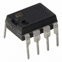
ST7FLITEU05B6 STMicroelectronics, ST7FLITEU05B6 Datasheet - Page 35

ST7FLITEU05B6
Manufacturer Part Number
ST7FLITEU05B6
Description
MCU 8BIT SGL VOLT FLASH 8-DIP
Manufacturer
STMicroelectronics
Series
ST7r
Datasheet
1.ST7FLITEU05M6.pdf
(139 pages)
Specifications of ST7FLITEU05B6
Core Processor
ST7
Core Size
8-Bit
Speed
8MHz
Peripherals
LVD, POR, PWM, WDT
Number Of I /o
5
Program Memory Size
2KB (2K x 8)
Program Memory Type
FLASH
Ram Size
128 x 8
Voltage - Supply (vcc/vdd)
2.4 V ~ 5.5 V
Data Converters
A/D 5x10b
Oscillator Type
Internal
Operating Temperature
-40°C ~ 85°C
Package / Case
8-DIP (0.300", 7.62mm)
Processor Series
ST7FLITEUx
Core
ST7
Data Bus Width
8 bit
Data Ram Size
128 B
Interface Type
ICC
Maximum Clock Frequency
4 MHz
Number Of Programmable I/os
5
Number Of Timers
2
Maximum Operating Temperature
+ 85 C
Mounting Style
Through Hole
Development Tools By Supplier
ST7FUS-PRIMER, ST7FLITE-SK/RAIS, ST7FLITU0-D/RAIS, STX-RLINK
Minimum Operating Temperature
- 40 C
On-chip Adc
10 bit, 5 Channel
For Use With
497-5858 - EVAL BOARD PLAYBACK ST7FLITE
Lead Free Status / RoHS Status
Lead free / RoHS Compliant
Eeprom Size
-
Connectivity
-
Lead Free Status / Rohs Status
Details
- Current page: 35 of 139
- Download datasheet (3Mb)
ST7LITEU05 ST7LITEU09
7.3
7.3.1
7.3.2
Note:
Register description
Main clock control/status register (MCCSR)
Reset value: 0000 0000 (00h)
Bits 7:2 = Reserved, must be kept cleared.
Bit 1 = MCO Main Clock Out enable bit
Bit 0 = SMS Slow mode selection bit
RC control register (RCCR)
Reset value: 1111 1111 (FFh)
Bits 7:0 = CR[9:2] RC oscillator frequency adjustment bits
To tune the oscillator, write a series of different values in the register until the correct
frequency is reached. The fastest method is to use a dichotomy starting with 80h.
CR9
This bit is read/write by software and cleared by hardware after a reset. This bit allows
to enable the MCO output clock.
0: MCO clock disabled, I/O port free for general purpose I/O.
1: MCO clock enabled.
This bit is read/write by software and cleared by hardware after a reset. This bit selects
the input clock f
0: Normal mode (f
1: Slow mode (f
These bits, as well as CR[1:0] bits in the SICSR register must be written immediately
after reset to adjust the RC oscillator frequency and to obtain the required accuracy.
The application can store the correct value for each voltage range in Flash memory and
write it to this register at start-up.
00h = maximum available frequency
FFh = lowest available frequency
7
0
7
CR8
0
OSC
CPU =
CPU =
or f
f
CR7
OSC
0
OSC
f
OSC
/32)
/32.
)
CR6
0
Read/write
Read/write
CR5
0
Supply, reset and clock management
CR4
0
MCO
CR3
CR2
SMS
0
0
35/139
Related parts for ST7FLITEU05B6
Image
Part Number
Description
Manufacturer
Datasheet
Request
R

Part Number:
Description:
KIT STARTER RAISONANCE ST7FLITE
Manufacturer:
STMicroelectronics
Datasheet:

Part Number:
Description:
STMicroelectronics [RIPPLE-CARRY BINARY COUNTER/DIVIDERS]
Manufacturer:
STMicroelectronics
Datasheet:

Part Number:
Description:
STMicroelectronics [LIQUID-CRYSTAL DISPLAY DRIVERS]
Manufacturer:
STMicroelectronics
Datasheet:

Part Number:
Description:
BOARD EVAL FOR MEMS SENSORS
Manufacturer:
STMicroelectronics
Datasheet:

Part Number:
Description:
NPN TRANSISTOR POWER MODULE
Manufacturer:
STMicroelectronics
Datasheet:

Part Number:
Description:
TURBOSWITCH ULTRA-FAST HIGH VOLTAGE DIODE
Manufacturer:
STMicroelectronics
Datasheet:

Part Number:
Description:
Manufacturer:
STMicroelectronics
Datasheet:

Part Number:
Description:
DIODE / SCR MODULE
Manufacturer:
STMicroelectronics
Datasheet:

Part Number:
Description:
DIODE / SCR MODULE
Manufacturer:
STMicroelectronics
Datasheet:

Part Number:
Description:
Search -----> STE16N100
Manufacturer:
STMicroelectronics
Datasheet:

Part Number:
Description:
Search ---> STE53NA50
Manufacturer:
STMicroelectronics
Datasheet:

Part Number:
Description:
NPN Transistor Power Module
Manufacturer:
STMicroelectronics
Datasheet:


