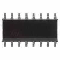
ST7FLITES2Y0M6 STMicroelectronics, ST7FLITES2Y0M6 Datasheet - Page 60

ST7FLITES2Y0M6
Manufacturer Part Number
ST7FLITES2Y0M6
Description
MCU 8BIT 1K FLASH 16SOIC
Manufacturer
STMicroelectronics
Series
ST7r
Datasheet
1.ST7FLITES2Y0B6.pdf
(124 pages)
Specifications of ST7FLITES2Y0M6
Core Processor
ST7
Core Size
8-Bit
Speed
8MHz
Connectivity
SPI
Peripherals
LVD, POR, PWM, WDT
Number Of I /o
13
Program Memory Size
1KB (1K x 8)
Program Memory Type
FLASH
Ram Size
128 x 8
Voltage - Supply (vcc/vdd)
2.4 V ~ 5.5 V
Oscillator Type
Internal
Operating Temperature
-40°C ~ 85°C
Package / Case
16-SOIC (3.9mm Width)
Controller Family/series
ST7
No. Of I/o's
13
Ram Memory Size
128Byte
Cpu Speed
8MHz
No. Of Timers
2
Embedded Interface Type
SPI
No. Of Pwm Channels
1
Rohs Compliant
Yes
Processor Series
ST7FLITESx
Core
ST7
Data Bus Width
8 bit
Data Ram Size
128 B
Interface Type
SPI
Maximum Clock Frequency
8 MHz
Number Of Programmable I/os
13
Number Of Timers
2
Operating Supply Voltage
2.4 V to 5.5 V
Maximum Operating Temperature
+ 85 C
Mounting Style
SMD/SMT
Development Tools By Supplier
ST7FLIT0-IND/USB, ST7FLITE-SK/RAIS, ST7MDT10-DVP3, ST7MDT10-EMU3, STX-RLINK
Minimum Operating Temperature
- 40 C
On-chip Adc
8 bit
For Use With
497-5858 - EVAL BOARD PLAYBACK ST7FLITE497-5049 - KIT STARTER RAISONANCE ST7FLITE
Lead Free Status / RoHS Status
Lead free / RoHS Compliant
Eeprom Size
-
Data Converters
-
Lead Free Status / Rohs Status
In Transition
Other names
497-4861
Available stocks
Company
Part Number
Manufacturer
Quantity
Price
ST7LITE0xY0, ST7LITESxY0
SERIAL PERIPHERAL INTERFACE (Cont’d)
11.3.3.1 Functional Description
A basic example of interconnections between a
single master and a single slave is illustrated in
Figure
The MOSI pins are connected together and the
MISO pins are connected together. In this way
data is transferred serially between master and
slave (most significant bit first).
The communication is always initiated by the mas-
ter. When the master device transmits data to a
slave device via MOSI pin, the slave device re-
Figure 38. Single Master/ Single Slave Application
60/124
1
38.
MSBit
8-BIT SHIFT REGISTER
GENERATOR
CLOCK
SPI
MASTER
LSBit
MOSI
SCK
SS
MISO
+5V
sponds by sending data to the master device via
the MISO pin. This implies full duplex communica-
tion with both data out and data in synchronized
with the same clock signal (which is provided by
the master device via the SCK pin).
To use a single data line, the MISO and MOSI pins
must be connected at each node (in this case only
simplex communication is possible).
Four possible data/clock timing relationships may
be chosen (see
must be programmed with the same timing mode.
MOSI
MISO
SCK
SS
Figure
8-BIT SHIFT REGISTER
MSBit
Not used if SS is managed
by software
41) but master and slave
SLAVE
LSBit


