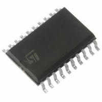
ST7FLITE39F2M6 STMicroelectronics, ST7FLITE39F2M6 Datasheet - Page 60

ST7FLITE39F2M6
Manufacturer Part Number
ST7FLITE39F2M6
Description
IC MCU 8BIT 8K FLASH 20SOIC
Manufacturer
STMicroelectronics
Series
ST7r
Datasheet
1.ST7FLITE35F2M6TR.pdf
(173 pages)
Specifications of ST7FLITE39F2M6
Core Processor
ST7
Core Size
8-Bit
Speed
16MHz
Connectivity
LINSCI, SPI
Peripherals
LVD, POR, PWM, WDT
Number Of I /o
15
Program Memory Size
8KB (8K x 8)
Program Memory Type
FLASH
Eeprom Size
256 x 8
Ram Size
384 x 8
Voltage - Supply (vcc/vdd)
2.7 V ~ 5.5 V
Data Converters
A/D 7x10b
Oscillator Type
Internal
Operating Temperature
-40°C ~ 85°C
Package / Case
20-SOIC (7.5mm Width)
Processor Series
ST7FLITE3x
Core
ST7
Data Bus Width
8 bit
Data Ram Size
384 B
Interface Type
LINSCI, SPI
Maximum Clock Frequency
8 MHz
Number Of Programmable I/os
15
Number Of Timers
4
Maximum Operating Temperature
+ 85 C
Mounting Style
SMD/SMT
Development Tools By Supplier
ST7FLITE-SK/RAIS, ST7MDT10-DVP3, ST7MDT10-EMU3, STX-RLINK
Minimum Operating Temperature
- 40 C
On-chip Adc
10 bit, 7 Channel
For Use With
497-8406 - BOARD STF20NM50FD/STF7LITE39BF2497-8403 - BOARD DEMO STCC08 AC SW DETECTOR497-6398 - BOARD EVAL ST7FLITE39/STM1403497-5858 - EVAL BOARD PLAYBACK ST7FLITE497-5514 - EVAL BOARD THERMO CONTROL REFRIG497-5049 - KIT STARTER RAISONANCE ST7FLITE
Lead Free Status / RoHS Status
Lead free / RoHS Compliant
Other names
497-5641-5
STFLITE39F2M6
STFLITE39F2M6
Available stocks
Company
Part Number
Manufacturer
Quantity
Price
ST7LITE3xF2
DUAL 12-BIT AUTORELOAD TIMER 3 (Cont’d)
Dead Time Generation
A dead time can be inserted between PWM0 and
PWM1 using the DTGR register. This is required
for half-bridge driving where PWM signals must
not be overlapped. The non-overlapping PWM0/
PWM1 signals are generated through a program-
mable dead time by setting the DTE bit.
Dead time value = DT[6:0] x Tcounter1
DTGR[7:0] is buffered inside so as to avoid de-
forming the current PWM cycle. The DTGR effect
will take place only after an overflow.
Figure 39. Dead Time Generation
In the above example, when the DTE bit is set:
– PWM goes low at DCR0 match and goes high at
– PWM1 goes high at DCR0+Tdt and goes low at
60/173
1
ATR1+Tdt
ATR match.
CK_CNTR1
CNTR1
PWM 1
PWM 0
PWM 0
PWM 1
counter = DCR0
DCR0
DCR0+1
T
counter1
T
dt
counter = DCR1
OVF
Notes:
1. Dead time is generated only when DTE=1 and
DT[6:0] ≠ 0. If DTE is set and DT[6:0]=0, PWM out-
put signals will be at their reset state.
2. Half Bridge driving is possible only if polarities of
PWM0 and PWM1 are not inverted, i.e. if OP0 and
OP1 are not set. If polarity is inverted, overlapping
PWM0/PWM1 signals will be generated.
With this programmable delay (Tdt), the PWM0
and PWM1 signals which are generated are not
overlapped.
T
dt
= DT[6:0] x T
ATR1
counter1
T
dt


