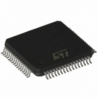
ST7FMC2R7T6 STMicroelectronics, ST7FMC2R7T6 Datasheet - Page 149

ST7FMC2R7T6
Manufacturer Part Number
ST7FMC2R7T6
Description
MCU 8BIT 48K FLASH 64TQFP
Manufacturer
STMicroelectronics
Series
ST7r
Datasheet
1.ST7FMC2S4T6.pdf
(309 pages)
Specifications of ST7FMC2R7T6
Core Processor
ST7
Core Size
8-Bit
Speed
8MHz
Connectivity
LINSCI, SPI
Peripherals
LVD, Motor Control PWM, POR, PWM, WDT
Number Of I /o
44
Program Memory Size
48KB (48K x 8)
Program Memory Type
FLASH
Ram Size
1.5K x 8
Voltage - Supply (vcc/vdd)
3.8 V ~ 5.5 V
Data Converters
A/D 16x10b
Oscillator Type
Internal
Operating Temperature
-40°C ~ 85°C
Package / Case
64-TQFP, 64-VQFP
Processor Series
ST7FMC2x
Core
ST7
Data Bus Width
8 bit
Data Ram Size
1536 B
Interface Type
SCI, SPI
Maximum Clock Frequency
8 MHz
Number Of Programmable I/os
60
Number Of Timers
5
Operating Supply Voltage
4.5 V to 5.5 V
Maximum Operating Temperature
+ 85 C
Mounting Style
SMD/SMT
Development Tools By Supplier
ST7MC-KIT/BLDC, ST7MDT50-EMU3, STX-RLINK
Minimum Operating Temperature
- 40 C
On-chip Adc
10 bit
For Use With
497-8402 - BOARD EVAL COMPLETE INVERTER497-8400 - KIT IGBT PWR MODULE CTRL ST7MC497-6408 - BOARD EVAL BLDC SENSORLESS MOTOR497-4734 - EVAL KIT 3KW POWER DRIVER BOARD497-4733 - EVAL KIT 1KW POWER DRIVER BOARD497-4732 - EVAL KIT 300W POWER DRIVER BOARD497-4731 - EVAL KIT PWR DRIVER CONTROL BRD
Lead Free Status / RoHS Status
Lead free / RoHS Compliant
Eeprom Size
-
Lead Free Status / Rohs Status
Details
Other names
497-4869
Available stocks
Company
Part Number
Manufacturer
Quantity
Price
Company:
Part Number:
ST7FMC2R7T6
Manufacturer:
STMicroelectronics
Quantity:
10 000
Company:
Part Number:
ST7FMC2R7T6TR
Manufacturer:
STMicroelectronics
Quantity:
10 000
- Current page: 149 of 309
- Download datasheet (6Mb)
MOTOR CONTROLLER (Cont’d)
10.6.6.2 Sensorless Mode
This mode is used to detect BEMF zero crossing
and end of demagnetization events.
The analog phase multiplexer connects the non-
excited motor winding to an analog 100mV hyster-
esis comparator referred to a selectable reference
voltage.
IS[1:0] bits in MPHST register allow to select the
input which will be drive to the comparator (either
MCIA, B or C). Be careful that the comparator is
OFF until CKE and/or DAC bit are set in MCRA
register.
The VR[2:0] bits in the MCRC register select the
reference voltage from seven internal values de-
pending on the noise level and the application volt-
age supply. The reference voltage can also be set
externally through the MCVREF pin when the
VR[2:0] bits are set.
Table 25. Threshold voltage setting
*Typical value for V
BEMF detections are performed during the meas-
urement window, when the excited windings are
free-wheeling through the low side switches and
diodes. At this stage the common star connection
VR2
1
1
1
1
0
0
0
0
VR1
1
1
0
0
1
1
0
0
VR0
1
0
1
0
1
0
1
0
DD
=5V.
Vref voltage threshold
Threshold voltage set by
external MCVREF pin
3.5V*
2.5V*
1.5V*
0.6V*
0.2V*
2V*
1V*
voltage is near to ground voltage (instead of V
when the excited windings are powered) and the
complete BEMF voltage is present on the non-ex-
cited winding terminal, referred to the ground ter-
minal.
The zero crossing sampling frequency is then de-
fined, in current mode, by the measurement win-
dow generator frequency (SA[3:0] bits in the
MPRSR register) or, in voltage mode, by the PWM
generator frequency and phase U duty cycle.
During a short period after a phase commutation
(C event), the winding where the back-emf will be
read is no longer excited but needs a demagneti-
sation phase during which the BEMF cannot be
read. A demagnetization current goes through the
free-wheeling diodes and the winding voltage is
stuck at the high voltage or to the ground terminal.
For this reason an “end of demagnetization event”
D must be detected on the winding before the de-
tector can sense a BEMF zero crossing.
For the end-of-demagnetization detection, no spe-
cial PWM configuration is needed, the comparator
sensing is done at a selectable frequency (f
see
So, the three events: C (commutation), D (demag-
netization) and Z (BEMF zero crossing) must al-
ways occur in this order in autoswitched mode
when hard commutation is selected.
The comparator output is processed by a detector
that automatically recognizes the D or Z event, de-
pending on the CPB or ZVD edge and level config-
uration bits as described in
To avoid wrong detection of D and Z events, a
blanking window filter is implemented for spike fil-
tering. In addition, by means of an event counter,
software can filter several consecutive events up
to a programmed limit before generating the D or Z
event internally. This is shown in
Figure
Table
80.
82.
ST7MC1xx/ST7MC2xx
Table
30.
Figure 79
149/309
SCF
DD
and
/2
),
1
Related parts for ST7FMC2R7T6
Image
Part Number
Description
Manufacturer
Datasheet
Request
R

Part Number:
Description:
STMicroelectronics [RIPPLE-CARRY BINARY COUNTER/DIVIDERS]
Manufacturer:
STMicroelectronics
Datasheet:

Part Number:
Description:
STMicroelectronics [LIQUID-CRYSTAL DISPLAY DRIVERS]
Manufacturer:
STMicroelectronics
Datasheet:

Part Number:
Description:
BOARD EVAL FOR MEMS SENSORS
Manufacturer:
STMicroelectronics
Datasheet:

Part Number:
Description:
NPN TRANSISTOR POWER MODULE
Manufacturer:
STMicroelectronics
Datasheet:

Part Number:
Description:
TURBOSWITCH ULTRA-FAST HIGH VOLTAGE DIODE
Manufacturer:
STMicroelectronics
Datasheet:

Part Number:
Description:
Manufacturer:
STMicroelectronics
Datasheet:

Part Number:
Description:
DIODE / SCR MODULE
Manufacturer:
STMicroelectronics
Datasheet:

Part Number:
Description:
DIODE / SCR MODULE
Manufacturer:
STMicroelectronics
Datasheet:

Part Number:
Description:
Search -----> STE16N100
Manufacturer:
STMicroelectronics
Datasheet:

Part Number:
Description:
Search ---> STE53NA50
Manufacturer:
STMicroelectronics
Datasheet:

Part Number:
Description:
NPN Transistor Power Module
Manufacturer:
STMicroelectronics
Datasheet:

Part Number:
Description:
DIODE / SCR MODULE
Manufacturer:
STMicroelectronics
Datasheet:


