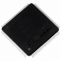
STR731FV1T6 STMicroelectronics, STR731FV1T6 Datasheet - Page 43

STR731FV1T6
Manufacturer Part Number
STR731FV1T6
Description
MCU 32BIT 128K FLASH 100-TQFP
Manufacturer
STMicroelectronics
Series
STR7r
Datasheet
1.STR735FZ2T7.pdf
(52 pages)
Specifications of STR731FV1T6
Core Processor
ARM7
Core Size
32-Bit
Speed
36MHz
Connectivity
CAN, I²C, SPI, UART/USART
Peripherals
DMA, POR, PWM, WDT
Number Of I /o
72
Program Memory Size
128KB (128K x 8)
Program Memory Type
FLASH
Ram Size
16K x 8
Voltage - Supply (vcc/vdd)
4.5 V ~ 5.5 V
Data Converters
A/D 12x10b
Oscillator Type
Internal
Operating Temperature
-40°C ~ 85°C
Package / Case
100-TQFP, 100-VQFP
Processor Series
STR731x
Core
ARM7TDMI
Data Bus Width
32 bit
Data Ram Size
16 KB
Interface Type
CAN, I2C, SPI, UART
Maximum Clock Frequency
36 MHz
Number Of Programmable I/os
72
Number Of Timers
9
Maximum Operating Temperature
+ 85 C
Mounting Style
SMD/SMT
3rd Party Development Tools
EWARM, EWARM-BL, MCBSTR730, KSK-STR731-PL, MDK-ARM, RL-ARM, ULINK2
Development Tools By Supplier
STR730-SK/HIT, STR730-SK/RAIS, STR731-SK/IAR, STR730-EVAL, STX-PRO/RAIS, STX-RLINK, STR79-RVDK/CPP, STR79-RVDK, STR79-RVDK/UPG
Minimum Operating Temperature
- 40 C
On-chip Adc
10 bit, 12 Channel
Lead Free Status / RoHS Status
Lead free / RoHS Compliant
Eeprom Size
-
Lead Free Status / Rohs Status
Details
Available stocks
Company
Part Number
Manufacturer
Quantity
Price
Company:
Part Number:
STR731FV1T6
Manufacturer:
STM
Quantity:
59
Company:
Part Number:
STR731FV1T6
Manufacturer:
STMicroelectronics
Quantity:
10 000
STR73xFxx
4.3.6
10-bit ADC characteristics
Subject to general operating conditions for V
Table 26.
1. Unless otherwise specified, typical data are based on T
2. Calibration is recommended once after each power-up.
3. During the sample time the input capacitance C
Symbol
t
t
C
f
CAL
CONV
I
V
t
ADC
ADC
as design guidelines and are not tested.
source. The internal resistance of the analog source must allow the capacitance to reach its final voltage
level within t
the conversion result. Values for the sample clock t
I
ADC
S
AIN
lkg
3)
2)
Conversion voltage range
Negative input leakage current on
analog pins
Internal sample and hold
capacitor
Calibration time
Sampling time
Total conversion time (including
sampling time)
Running mode
Power-down mode
ADC characteristics
S.
After the end of the sample time t
Parameter
2)
AIN
S
V
µA on adjacent
analog pin
f
f
f
ADC
ADC
ADC
, changes of the analog input voltage have no effect on
IN
S
(6.8 max) can be charged/discharged by the external
DDA
<
Normal mode
depend on programming.
V
Conditions
= 10 MHz
= 10 MHz
= 10 MHz
SS,
A
, f
=25°C and V
MCLK
| I
IN
|< 400
, and T
DDA
-V
A
30 (10 for sampling
+20 for successive
approximation)
V
Min
0.4
unless otherwise specified.
SS
SSA
1
3
=5.0V. They are given only
Electrical parameters
Typ
580.2
5802
5
1)
14
V
Max
3.5
10
DDA
6
5
1
1/f
1/f
MHz
Unit
mA
μA
μA
pF
µs
µs
µs
43/52
V
ADC
ADC


