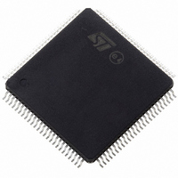
ST10F272Z2T3 STMicroelectronics, ST10F272Z2T3 Datasheet - Page 33

ST10F272Z2T3
Manufacturer Part Number
ST10F272Z2T3
Description
MCU 16BIT 256KBIT FLASH 144-TQFP
Manufacturer
STMicroelectronics
Series
ST10r
Datasheet
1.ST10F272Z2Q3.pdf
(189 pages)
Specifications of ST10F272Z2T3
Core Processor
ST10
Core Size
16-Bit
Speed
40MHz
Connectivity
ASC, CAN, EBI/EMI, I²C, SSC, UART/USART
Peripherals
POR, PWM, WDT
Number Of I /o
111
Program Memory Size
256KB (256K x 8)
Program Memory Type
FLASH
Ram Size
20K x 8
Voltage - Supply (vcc/vdd)
4.5 V ~ 5.5 V
Data Converters
A/D 24x10b
Oscillator Type
Internal
Operating Temperature
-40°C ~ 125°C
Package / Case
144-TQFP, 144-VQFP
Lead Free Status / RoHS Status
Lead free / RoHS Compliant
Eeprom Size
-
Available stocks
Company
Part Number
Manufacturer
Quantity
Price
Company:
Part Number:
ST10F272Z2T3
Manufacturer:
STMicroelectronics
Quantity:
10 000
- Current page: 33 of 189
- Download datasheet (4Mb)
ST10F272Z2
5.4.4
5.4.5
Flash control register 1 high
The Flash Control Register 1 High (FCR1H), together with Flash Control Register 1 Low
(FCR1L), is used to select the Sectors to Erase, or during any write operation to monitor the
status of each Sector and Bank.
FCR1H (0x08 0006)
Table 11.
During any erase operation, this bit is automatically set and gives the status of the Bank 0.
The meaning of B0Fy bit for Sector y of Bank 0 is given by the next Table 4 Banks (BxS) and
Sectors (BxFy) Status bits meaning. These bits are automatically reset at the end of an
erase operation if no errors are detected.
Table 12.
Flash data register 0 low
The Flash Address Registers (FARH/L) and the Flash Data Registers (FDR1H/L-FDR0H/L)
are used during the program operations to store Flash Address in which to program and
Data to program.
FDR0L (0x08 0008)
Table 13.
DIN15 DIN14 DIN13 DIN12 DIN11 DIN10 DIN9 DIN8 DIN7 DIN6 DIN5 DIN4 DIN3 DIN2 DIN1 DIN0
B0S
DIN(15:0)
RW
ERR
15
15
1
0
0
Bit
Bit
RW
14
14
SUSP
1
0
-
Banks (BxS) and sectors (BxFy) status bits meaning
RW
13
13
Flash control register 1 high
Flash data register 0 low
Erase Error in Bank 0
Erase Suspended in Bank 0
Don’t care
reserved
Bank 0 Status (IFLASH)
During any erase operation, this bit is automatically modified and gives the status
of the Bank 0. The meaning of B0S bit is given in the next Table 4 Banks (BxS) and
Sectors (BxFy) Status bits meaning. This bit is automatically reset at the end of a
erase operation if no errors are detected.
Data Input 15:0
These bits must be written with the Data to program the Flash with the following
operations: Word Program (32-bit), Double Word Program (64-bit) and Set
Protection.
RW
12
12
RW
11
11
B0S = 1 meaning
RW
10
10
RW
9
9
FCR
FCR
B0S
RW
RS
8
8
RW
7
7
Function
Function
RW
Erase Error in Sector y of Bank 0
Erase Suspended in Sector y of Bank 0
Don’t care
6
6
RW
reserved
5
5
B0Fy = 1 meaning
RW
4
4
Internal Flash memory
RW
3
3
Reset value:
Reset value:
RW
2
2
RW
1
1
FFFFh
0000h
33/189
RW
0
0
Related parts for ST10F272Z2T3
Image
Part Number
Description
Manufacturer
Datasheet
Request
R

Part Number:
Description:
STMicroelectronics [RIPPLE-CARRY BINARY COUNTER/DIVIDERS]
Manufacturer:
STMicroelectronics
Datasheet:

Part Number:
Description:
STMicroelectronics [LIQUID-CRYSTAL DISPLAY DRIVERS]
Manufacturer:
STMicroelectronics
Datasheet:

Part Number:
Description:
BOARD EVAL FOR MEMS SENSORS
Manufacturer:
STMicroelectronics
Datasheet:

Part Number:
Description:
NPN TRANSISTOR POWER MODULE
Manufacturer:
STMicroelectronics
Datasheet:

Part Number:
Description:
TURBOSWITCH ULTRA-FAST HIGH VOLTAGE DIODE
Manufacturer:
STMicroelectronics
Datasheet:

Part Number:
Description:
Manufacturer:
STMicroelectronics
Datasheet:

Part Number:
Description:
DIODE / SCR MODULE
Manufacturer:
STMicroelectronics
Datasheet:

Part Number:
Description:
DIODE / SCR MODULE
Manufacturer:
STMicroelectronics
Datasheet:

Part Number:
Description:
Search -----> STE16N100
Manufacturer:
STMicroelectronics
Datasheet:

Part Number:
Description:
Search ---> STE53NA50
Manufacturer:
STMicroelectronics
Datasheet:

Part Number:
Description:
NPN Transistor Power Module
Manufacturer:
STMicroelectronics
Datasheet:


