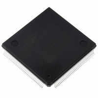
ST10F269Z2Q6 STMicroelectronics, ST10F269Z2Q6 Datasheet - Page 111

ST10F269Z2Q6
Manufacturer Part Number
ST10F269Z2Q6
Description
MCU 16BIT 256K FLASH 144PQFP
Manufacturer
STMicroelectronics
Series
ST10r
Specifications of ST10F269Z2Q6
Core Processor
ST10
Core Size
16-Bit
Speed
40MHz
Connectivity
CAN, EBI/EMI, SSC, UART/USART
Peripherals
POR, PWM, WDT
Number Of I /o
111
Program Memory Size
256KB (256K x 8)
Program Memory Type
FLASH
Ram Size
12K x 8
Voltage - Supply (vcc/vdd)
4.5 V ~ 5.5 V
Data Converters
A/D 16x10b
Oscillator Type
Internal
Operating Temperature
-40°C ~ 85°C
Package / Case
144-QFP
Controller Family/series
ST10
No. Of I/o's
111
Ram Memory Size
12KB
Cpu Speed
40MHz
No. Of Timers
5
Embedded Interface Type
CAN, SSC, USART
Rohs Compliant
Yes
Processor Series
ST10F26x
Core
ST10
Data Bus Width
16 bit
Data Ram Size
12 KB
Interface Type
CAN, SSC, USART
Maximum Clock Frequency
40 MHz
Number Of Programmable I/os
111
Number Of Timers
2 x 16 bit
Operating Supply Voltage
0.3 V to 4 V
Maximum Operating Temperature
+ 85 C
Mounting Style
SMD/SMT
Minimum Operating Temperature
- 40 C
On-chip Adc
16 bit x 10 bit
Lead Free Status / RoHS Status
Lead free / RoHS Compliant
Eeprom Size
-
Lead Free Status / Rohs Status
Details
Other names
497-4833
Available stocks
Company
Part Number
Manufacturer
Quantity
Price
Company:
Part Number:
ST10F269Z2Q6
Manufacturer:
ST
Quantity:
201
Company:
Part Number:
ST10F269Z2Q6
Manufacturer:
ST
Quantity:
745
Company:
Part Number:
ST10F269Z2Q6
Manufacturer:
STMicroelectronics
Quantity:
10 000
Part Number:
ST10F269Z2Q6
Manufacturer:
ST
Quantity:
20 000
ST10F269-T3
Unlike hardware and software resets, the watchdog reset completes a running external bus cycle if this
bus cycle either does not use READY, or if READY is sampled active (low) after the programmed wait
states. When READY is sampled inactive (high) after the programmed wait states the running external
bus cycle is aborted. Then the internal reset sequence (1024 TCL) is started. The microcontroller
behaviour is the same as for a short hardware reset, except that only P0.12...P0.6 bits are latched, while
previously latched values of P0.5...P0.2 are cleared.
18.5 - RSTOUT, RSTIN, Bidirectional Reset
18.5.1 - RSTOUT Pin
The RSTOUT pin is driven active (low level) at the beginning of any reset sequence (synchronous/
asynchronous hardware, software and watchdog timer resets). RSTOUT pin stays active low beyond the
end of the initialization routine, until the protected EINIT instruction (End of Initialization) is completed.
18.5.2 - Bidirectional Reset
The bidirectional reset function is enabled by setting SYSCON.BDRSTEN (bit 3). This function is disabled
by any reset sequence which always clears the SYSCON.BDRSTEN bit.
It can only be enabled during the initial is at ion routine, before EINIT instruction is completed.
If V
voltage drops below the RPD pin threshold (typically 2.5V for V
= 5V) when RSTIN pin is low or
RPD
DD
when RSTIN pin is internally pulled low, the ST10 reset circuitry disables the bidirectional reset function
and RSTIN pin is no more pulled low. The reset is processed as an asynchronous reset.
The bidirectional reset function is useful for external peripherals with on-chip memory because the reset
signal output on RSTIN pin is de-activated before the CPU starts its first instruction fetch.
18.5.3 - RSTIN pin
When the bidirectional reset function is enabled, the open-drain of the RSTIN pin is activated, pulling
down the reset signal, for the duration of the internal reset sequence. See Figure 56 and Figure 57. At the
end of the sequence the pull-down is released and the RSTIN pin gets back its input function.
The bidirectional reset function can be used:
– to convert SW or WD resets to a hardware reset so that the configuration can be (re-)latched from PORT0.
– to make visible SW or WDT resets at RSTIN pin whenever RSTIN is the only reset signal used by the
application (RSTOUT not used).
– to get a deactivated reset signal before CPU starts its first instruction fetch.
The configuration latched from PORT0 is determined by the kind of reset generated by the application.
(Refer to Table 29).
Converting a SW or WDT reset to a hardware reset allows the PLL to re-lock or the PLL configuration to
be re-latched, provided a SW or WDT reset is generated by the application program is case of PLL unlock
or input clock fail.
18.6 - Reset Circuitry
The internal reset circuitry is described in Figure 58.
An internal pull-up resistor is implemented on RSTIN pin. (50kΩ minimum, to 250kΩ maximum). The
minimum reset time must be calculated using the lowest value. In addition, a programmable pull-down
(SYSCON.BDRSTEN bit 3) drives the RSTIN pin according to the internal reset state. The RSTOUT pin
provides a signals to the application. (Refer to Section 18.5 - RSTOUT, RSTIN, Bidirectional Reset).
A weak internal pull-down is connected to the RPD pin to discharge external capacitor to V
at a rate of
SS
100µA to 200µA. This Pull-down is turned on when RSTIN pin is low
If bit PWDCFG of SYSCON register is set, an internal pull-up resistor is activated at the end of the reset
sequence. This pull-up charges the capacitor connected to RPD pin.
If the bidirectional reset function is not used, the simplest way to reset ST10F269-T3 is to connect
external components as shown in Figure 59. It works with reset from application (hardware or manual)
and with power-on. The value of C1 capacitor, connected on RSTIN pin with internal pull-up resistor
(50kΩ to 250kΩ), must lead to a charging time long enough to let the internal or external oscillator and / or
the on-chip PLL to stabilize.
111/162


