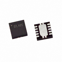
C8051F302-GMR Silicon Laboratories Inc, C8051F302-GMR Datasheet - Page 40

C8051F302-GMR
Manufacturer Part Number
C8051F302-GMR
Description
IC 8051 MCU 8K FLASH 11QFN
Manufacturer
Silicon Laboratories Inc
Series
C8051F30xr
Specifications of C8051F302-GMR
Core Processor
8051
Core Size
8-Bit
Speed
25MHz
Connectivity
SMBus (2-Wire/I²C), UART/USART
Peripherals
POR, PWM, Temp Sensor, WDT
Number Of I /o
8
Program Memory Size
8KB (8K x 8)
Program Memory Type
FLASH
Ram Size
256 x 8
Voltage - Supply (vcc/vdd)
2.7 V ~ 3.6 V
Data Converters
A/D 8x8b
Oscillator Type
External
Operating Temperature
-40°C ~ 85°C
Package / Case
11-VQFN
For Use With
336-1444 - ADAPTER PROGRAM TOOLSTICK F300
Lead Free Status / RoHS Status
Lead free / RoHS Compliant
Eeprom Size
-
Available stocks
Company
Part Number
Manufacturer
Quantity
Price
Company:
Part Number:
C8051F302-GMR
Manufacturer:
SiliconL
Quantity:
3 000
Company:
Part Number:
C8051F302-GMR
Manufacturer:
SILICON
Quantity:
5 000
Part Number:
C8051F302-GMR
Manufacturer:
SILICONLABS/èٹ¯ç§‘
Quantity:
20 000
C8051F300/1/2/3/4/5
5.3.2. Tracking Modes
According to Table 5.1 on page 47, each ADC0 conversion must be preceded by a minimum tracking time
for the converted result to be accurate. The AD0TM bit in register ADC0CN controls the ADC0 track-and-
hold mode. In its default state, the ADC0 input is continuously tracked except when a conversion is in prog-
ress. When the AD0TM bit is logic 1, ADC0 operates in low-power track-and-hold mode. In this mode,
each conversion is preceded by a tracking period of 3 SAR clocks (after the start-of-conversion signal).
When the CNVSTR signal is used to initiate conversions in low-power tracking mode, ADC0 tracks only
when CNVSTR is low; conversion begins on the rising edge of CNVSTR (see Figure 5.4). Tracking can
also be disabled (shutdown) when the device is in low power standby or sleep modes. Low-power track-
and-hold mode is also useful when AMUX or PGA settings are frequently changed, due to the settling time
requirements described in
40
Timer 0, Timer 2, Timer 1 Overflow
(AD0CM[2:0]=000, 001, 010, 011)
Write '1' to AD0BUSY,
Figure 5.4. 8-Bit ADC Track and Conversion Example Timing
(AD0CM[2:0]=1xx)
SAR Clocks
AD0TM=1
AD0TM=0
AD0TM=1
AD0TM=0
CNVSTR
Section “5.3.3. Settling Time Requirements” on page
Clocks
Clocks
SAR
SAR
Low Power
or Convert
Low Power
or Convert
Track or
Convert
A. ADC Timing for External Trigger Source
Track or Convert
B. ADC Timing for Internal Trigger Source
1
1
Rev. 2.9
Track
2
2
Track
3
3
4
4
1
5
5
Convert
2
6
6
3
7
7
4
8
8
Convert
5
9
9
Convert
Convert
10
6
10
7
11 12
11 12
8
9
13
41.
10
14 15
11 12
Track
Low Power
Low Power
Mode
Mode
Track


