C8051F34C-GQ Silicon Laboratories Inc, C8051F34C-GQ Datasheet
C8051F34C-GQ
Manufacturer Part Number
C8051F34C-GQ
Description
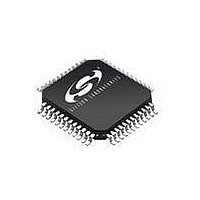
IC 8051 MCU 64K FLASH 48TQFP
Manufacturer
Silicon Laboratories Inc
Series
C8051F34xr
Specifications of C8051F34C-GQ
Program Memory Type
FLASH
Program Memory Size
64KB (64K x 8)
Package / Case
48-TQFP, 48-VQFP
Core Processor
8051
Core Size
8-Bit
Speed
48MHz
Connectivity
EBI/EMI, SMBus (2-Wire/I²C), SPI, UART/USART, USB
Peripherals
Brown-out Detect/Reset, POR, PWM, WDT
Number Of I /o
40
Ram Size
4.25K x 8
Voltage - Supply (vcc/vdd)
2.7 V ~ 5.25 V
Oscillator Type
Internal
Operating Temperature
-40°C ~ 85°C
Processor Series
C8051F3x
Core
8051
Data Ram Size
256 KB
Interface Type
UART
Maximum Clock Frequency
48 MHz
Number Of Programmable I/os
40
Number Of Timers
4
Operating Supply Voltage
2.7 V to 5.25 V
Maximum Operating Temperature
+ 85 C
Mounting Style
SMD/SMT
3rd Party Development Tools
KSK-SL-F34X, KSK-SL-TOOLSTICK, PK51, CA51, A51, ULINK2
Development Tools By Supplier
C8051F340DK
Minimum Operating Temperature
- 40 C
Lead Free Status / RoHS Status
Lead free / RoHS Compliant
Eeprom Size
-
Data Converters
-
Lead Free Status / Rohs Status
Lead free / RoHS Compliant
Available stocks
Company
Part Number
Manufacturer
Quantity
Price
Company:

Part Number:
C8051F34C-GQ
Manufacturer:
Silicon Laboratories Inc
Quantity:
10 000
Company:
Part Number:
C8051F34C-GQR
Manufacturer:
Silicon Laboratories Inc
Quantity:
10 000
Analog Peripherals
Two Comparators
POR/Brown-out Detector
USB Function Controller
-
-
-
-
-
-
On-Chip Debug
-
-
-
-
Temperature Range: –40 to +85 °C
USB
USB specification 2.0 compliant
Full-speed (12 Mbps) or low-speed (1.5 Mbps) operation
Integrated clock recovery; no external crystal required for either full-
speed or low-speed operation
Supports eight flexible endpoints
Dedicated 1 kB USB buffer memory
Integrated transceiver; no external resistors required
On-chip debug circuitry facilitates full speed, non-intrusive in-system
debug (no emulator required)
Provides breakpoints, single stepping
Inspect/modify memory, registers, and USB memory
Superior performance to emulation systems using ICE-chips, target
pods, and sockets
C2CK/RST
VREG
VBUS
GND
VDD
C2D
D+
D-
Power-On
Regulator
Monitor
Voltage
Supply
Reset
XTAL1
XTAL2
Reset
Power
Net
System Clock Setup
Transceiver
Oscillator
Oscillator
Recovery
External
Full / Low
Internal
Debug / Programming
64k Byte ISP FLASH
Clock
USB Peripheral
Speed
Controller Core
Program Memory
CIP-51 8051
256 Byte RAM
4k Byte XRAM
Hardware
Copyright © 2009 by Silicon Laboratories
Low Freq.
Oscillator
Controller
Multiplier
1k Byte
Clock
RAM
USB, 48 MIPS, 64 kB Flash, 48-Pin Mixed-Signal MCU
SFR
Bus
High-Speed 8051 µC Core
-
-
-
Memory
-
-
-
Digital Peripherals
-
-
-
-
Clock Sources
-
-
-
Voltage Regulator
-
-
Operating Voltage: 2.7 to 5.25 V
Ordering Part Number
-
Timers 0, 1,
PCA/WDT
Pipelined instruction architecture; executes 70% of instructions in 1 or 2
system clocks
Up to 48 MIPS throughput with 48 MHz Clock
Expanded interrupt handler
4352 bytes data RAM (256 + 4 kB)
64 kB Flash; in-system programmable in 512-byte sectors (512 bytes
are reserved)
External parallel data memory interface
40 port I/O; all are 5 V tolerant
Hardware SMBus™ (I
available concurrently
4 general-purpose 16-bit counter/timers
Programmable 16-bit counter array with 5 capture/compare modules
Internal oscillator: 0.25% accuracy with clock recovery enabled;
supports all USB and UART modes
External oscillator: Crystal, RC, C, or Clock
On-chip clock multiplier: up to 48 MHz
On-chip voltage regulator supports USB bus-powered operation
Regulator bypass mode supports USB self-powered operation
C8051F34C-GQ, 48-Pin TQFP, 9x9 mm
External Memory
Analog Peripherals
Digital Peripherals
UART0
UART1
SMBus
Port I/O Configuration
2, 3
SPI
Crossbar Control
Interface
Address
Control
Data
2 Comparators
Crossbar
Decoder
Priority
CP0
CP1
2
C™ compatible), SPI™, and 2 UART serial ports
P2 / P3
+
+
-
-
P1
P4
Drivers
Drivers
Drivers
Drivers
Drivers
Port 0
Port 1
Port 2
Port 3
Port 4
C8051F34C
2
P0.0
P0.1
P0.2
P0.3
P0.4
P0.5
P0.6/XTAL1
P0.7/XTAL2
P1.0
P1.1
P1.2
P1.3
P1.4/CNVSTR
P1.5/VREF
P1.6
P1.7
P2.0
P2.1
P2.2
P2.3
P2.4
P2.5
P2.6
P2.7
P3.0
P3.1
P3.2
P3.3
P3.4
P3.5
P3.6
P3.7
P4.0
P4.1
P4.2
P4.3
P4.4
P4.5
P4.6
P4.7
9.24.2009
Related parts for C8051F34C-GQ
Image
Part Number
Description
Manufacturer
Datasheet
Request
R

Part Number:
Description:
SMD/C�/SINGLE-ENDED OUTPUT SILICON OSCILLATOR
Manufacturer:
Silicon Laboratories Inc
Part Number:
Description:
Manufacturer:
Silicon Laboratories Inc
Datasheet:
Part Number:
Description:
N/A N/A/SI4010 AES KEYFOB DEMO WITH LCD RX
Manufacturer:
Silicon Laboratories Inc
Datasheet:
Part Number:
Description:
N/A N/A/SI4010 SIMPLIFIED KEY FOB DEMO WITH LED RX
Manufacturer:
Silicon Laboratories Inc
Datasheet:
Part Number:
Description:
N/A/-40 TO 85 OC/EZLINK MODULE; F930/4432 HIGH BAND (REV E/B1)
Manufacturer:
Silicon Laboratories Inc
Part Number:
Description:
EZLink Module; F930/4432 Low Band (rev e/B1)
Manufacturer:
Silicon Laboratories Inc
Part Number:
Description:
I�/4460 10 DBM RADIO TEST CARD 434 MHZ
Manufacturer:
Silicon Laboratories Inc
Part Number:
Description:
I�/4461 14 DBM RADIO TEST CARD 868 MHZ
Manufacturer:
Silicon Laboratories Inc
Part Number:
Description:
I�/4463 20 DBM RFSWITCH RADIO TEST CARD 460 MHZ
Manufacturer:
Silicon Laboratories Inc
Part Number:
Description:
I�/4463 20 DBM RADIO TEST CARD 868 MHZ
Manufacturer:
Silicon Laboratories Inc
Part Number:
Description:
I�/4463 27 DBM RADIO TEST CARD 868 MHZ
Manufacturer:
Silicon Laboratories Inc
Part Number:
Description:
I�/4463 SKYWORKS 30 DBM RADIO TEST CARD 915 MHZ
Manufacturer:
Silicon Laboratories Inc
Part Number:
Description:
N/A N/A/-40 TO 85 OC/4463 RFMD 30 DBM RADIO TEST CARD 915 MHZ
Manufacturer:
Silicon Laboratories Inc
Part Number:
Description:
I�/4463 20 DBM RADIO TEST CARD 169 MHZ
Manufacturer:
Silicon Laboratories Inc