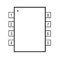
MAXQ610A-0000+ Maxim Integrated Products, MAXQ610A-0000+ Datasheet - Page 6

MAXQ610A-0000+
Manufacturer Part Number
MAXQ610A-0000+
Description
IC MCU 16BIT 64K IR MOD 32TQFN
Manufacturer
Maxim Integrated Products
Series
MAXQ™r
Datasheets
1.MAXQ610A-0000.pdf
(28 pages)
2.MAXQ610A-0000.pdf
(29 pages)
3.MAXQ610A-0000.pdf
(23 pages)
Specifications of MAXQ610A-0000+
Core Processor
RISC
Core Size
16-Bit
Speed
12MHz
Connectivity
SPI, UART/USART
Peripherals
Brown-out Detect/Reset, Infrared, Power-Fail, POR, WDT
Number Of I /o
20
Program Memory Size
64KB (64K x 8)
Program Memory Type
FLASH
Ram Size
2K x 8
Voltage - Supply (vcc/vdd)
1.7 V ~ 3.6 V
Oscillator Type
Internal
Operating Temperature
0°C ~ 70°C
Package / Case
32-TQFN Exposed Pad
Processor Series
MAXQ610
Core
RISC
Data Bus Width
16 bit
Data Ram Size
2 KB
Interface Type
SPI, USART
Maximum Clock Frequency
12 MHz
Number Of Timers
4
Operating Supply Voltage
1.7 V to 3.6 V
Maximum Operating Temperature
+ 70 C
Mounting Style
SMD/SMT
Minimum Operating Temperature
0 C
Controller Family/series
MAXQ
No. Of I/o's
24
Ram Memory Size
2048Byte
Cpu Speed
12MHz
No. Of Timers
2
Embedded Interface Type
JTAG, SPI, USART
Rohs Compliant
Yes
Number Of Programmable I/os
32
Development Tools By Supplier
MAXQ610-KIT
Package
32TQFN EP
Family Name
MAXQ
Maximum Speed
12 MHz
Lead Free Status / RoHS Status
Lead free / RoHS Compliant
Eeprom Size
-
Data Converters
-
Lead Free Status / Rohs Status
Lead free / RoHS Compliant
Other names
90-M6800+B01
16-Bit Microcontroller with Infrared Module
RECOMMENDED DC OPERATING CONDITIONS (continued)
(V
Note 1:
Note 2:
Note 3:
Note 4:
Note 5:
Note 6:
Note 7:
Note 8:
Note 9:
Note 10: The maximum total current, I
Note 11: Programming time does not include overhead associated with utility ROM interface.
6
WAKE-UP TIMER
Wake-Up Timer Interval
FLASH MEMORY
System Clock During Flash
Programming/Erase
Flash Erase Time
Flash Programming Time per
Word
Write/Erase Cycles
Data Retention
IR
Carrier Frequency
DD
_______________________________________________________________________________________
= V
RST
PARAMETER
Specifications to 0°C are guaranteed by design and are not production tested.
It is not recommended to write to flash memory when the supply voltage drops below the power-fail warning levels as
there is uncertainty in the duration of continuous power supply. The user application should check the status of the power-
fail warning flag before writing to flash to ensure complete write operations.
The power-fail warning monitor and the power-fail reset monitor track each other with a minimum delta between the two of
0.11V.
The power-fail reset and power-on-reset (POR) detectors operate in tandem to ensure that one or both signals are active
at all times when V
achieved.
Guaranteed by design and not production tested.
Measured on the V
any current. Part is executing code from flash memory.
The power-check interval (PCI) can be set to always on, 1024, 2048, or 4096 nanopower ring oscillator clock cycles.
Current consumption during POR when powering up while V
The minimum amount of time that V
the maximum specified voltage drop. This does not include the IRTX output.
to 3.6V, T
A
= 0°C to +70°C.) (Note 1)
DD
DD
< V
pin and the part not in reset. All inputs are connected to GND or V
RST
f
SYMBOL
FPSYSCLK
t
WAKEUP
t
t
OH
ERASE
. Doing so ensures the device maintains the reset state until the minimum operating voltage is
PROG
t
f
ME
IR
(max) and I
DD
must be below V
Mass erase
Page erase
(Note 11)
T
(Note 5)
A
= +25°C
OL
(max), for all listed outputs combined should not exceed 32mA to satisfy
CONDITIONS
PFW
before a power-fail event is detected.
DD
< V
POR
.
1/f
20,000
MIN
100
NANO
20
20
20
DD
5
. Outputs do not source/sink
TYP
65,535/
f
NANO
MAX
f
CK
100
40
40
/2
Cycles
UNITS
Years
MHz
ms
Hz
μs
s


