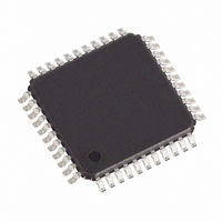
DS80C323-ECD+ Maxim Integrated Products, DS80C323-ECD+ Datasheet - Page 4

DS80C323-ECD+
Manufacturer Part Number
DS80C323-ECD+
Description
IC MCU HI SPEED 18MHZ 44-TQFP
Manufacturer
Maxim Integrated Products
Series
80Cr
Datasheet
1.DS80C323-QND.pdf
(38 pages)
Specifications of DS80C323-ECD+
Core Processor
8051
Core Size
8-Bit
Speed
18MHz
Connectivity
EBI/EMI, SIO, UART/USART
Peripherals
Power-Fail Reset, WDT
Number Of I /o
32
Program Memory Type
ROMless
Ram Size
256 x 8
Voltage - Supply (vcc/vdd)
4.5 V ~ 5.5 V
Oscillator Type
External
Operating Temperature
0°C ~ 70°C
Package / Case
44-TQFP, 44-VQFP
Processor Series
80C
Core
8051
Data Bus Width
8 bit
Program Memory Size
64 KB
Data Ram Size
64 KB
Interface Type
UART
Maximum Clock Frequency
18 MHz
Number Of Programmable I/os
32
Number Of Timers
3
Operating Supply Voltage
5 V
Maximum Operating Temperature
+ 70 C
Mounting Style
SMD/SMT
3rd Party Development Tools
PK51, CA51, A51, ULINK2
Minimum Operating Temperature
0 C
Package
44TQFP
Device Core
8051
Family Name
80C
Maximum Speed
18 MHz
Lead Free Status / RoHS Status
Lead free / RoHS Compliant
Eeprom Size
-
Program Memory Size
-
Data Converters
-
Lead Free Status / Rohs Status
Lead free / RoHS Compliant
Other names
DS80C323+ECD
DS80C323+ECD
DS80C323+ECD
PIN DESCRIPTION (continued)
DIP
1–8
30
39
38
37
36
35
34
33
32
PLCC
2–9
33
43
42
41
40
39
38
37
36
PIN
40–44,
TQFP
1–3
27
37
36
35
34
33
32
31
30
P1.0–P1.7
NAME
ALE
AD0
AD1
AD2
AD3
AD4
AD5
AD6
AD7
Address Latch-Enable Output. This pin functions as a clock to latch
the external address LSB from the multiplexed address/data bus. This
signal is commonly connected to the latch enable of an external 373
family transparent latch. ALE has a pulse width of 1.5 XTAL1 cycles
and a period of four XTAL1 cycles. ALE is forced high when the
device is in a reset condition.
Port 0, Input/Output. Port 0 is the multiplexed address/data bus.
During the time when ALE is high, the LSB of a memory address is
presented. When ALE falls, the port transitions to a bidirectional data
bus. This bus is used to read external ROM and read/write external
RAM memory or peripherals. The Port 0 has no true port latch and
cannot be written directly by software. The reset condition of Port 0 is
high. No pullup resistors are needed.
Port 1, I/O. Port 1 functions as both an 8-bit, bidirectional I/O port and
an alternate functional interface for Timer 2 I/O, new External
Interrupts, and new Serial Port 1. The reset condition of Port 1 is with
all bits at logic 1. In this state, a weak pullup holds the port high. This
condition also serves as an input mode, since any external circuit that
writes to the port will overcome the weak pullup. When software writes
a 0 to any port pin, the device will activate a strong pulldown that
remains on until either a 1 is written or a reset occurs. Writing a 1 after
the port has been at 0 will cause a strong transition driver to turn on,
followed by a weaker sustaining pullup. Once the momentary strong
driver turns off, the port once again becomes the output high (and
input) state. The alternate modes of Port 1 are outlined as follows:
DIP
1
2
3
4
5
6
7
8
PLCC
PIN
DS80C320/DS80C323 High-Speed/Low-Power Microcontrollers
2
3
4
5
6
7
8
9
4 of 38
TQFP
40
41
42
43
44
1
2
3
PORT
P1.0
P1.1
P1.2
P1.3
P1.4
P1.5
P1.6
P1.7
FUNCTION
ALTERNATE
RXD1
T2EX
TXD1
INT2
INT3
INT4
INT5
T2
External I/O for
Timer/Counter 2
Timer/Counter 2
Capture/Reload Trigger
Serial Port 1 Input
Serial Port 1 Output
External Interrupt 2
(Positive-Edge Detect)
External Interrupt 3
(Negative-Edge Detect)
External Interrupt 4
(Positive-Edge Detect)
External Interrupt 5
(Negative-Edge Detect)
FUNCTION


