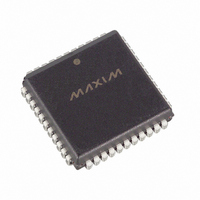
DS89C450-QNG+ Maxim Integrated Products, DS89C450-QNG+ Datasheet - Page 31

DS89C450-QNG+
Manufacturer Part Number
DS89C450-QNG+
Description
IC MCU FLASH 64KB 25MHZ 44-PLCC
Manufacturer
Maxim Integrated Products
Series
89Cr
Datasheet
1.DS89C450-KIT.pdf
(46 pages)
Specifications of DS89C450-QNG+
Core Processor
8051
Core Size
8-Bit
Speed
25MHz
Connectivity
EBI/EMI, SIO, UART/USART
Peripherals
Power-Fail Reset, WDT
Number Of I /o
32
Program Memory Size
64KB (64K x 8)
Program Memory Type
FLASH
Ram Size
1K x 8
Voltage - Supply (vcc/vdd)
4.5 V ~ 5.5 V
Oscillator Type
External
Operating Temperature
-40°C ~ 85°C
Package / Case
44-LCC, 44-PLCC
Processor Series
DS89C450
Core
8051
Data Bus Width
8 bit
Data Ram Size
1 KB
Interface Type
UART
Maximum Clock Frequency
33 MHz
Number Of Programmable I/os
4
Number Of Timers
3
Operating Supply Voltage
4.5 V to 5.5 V
Maximum Operating Temperature
+ 85 C
Mounting Style
SMD/SMT
3rd Party Development Tools
PK51, CA51, A51, ULINK2
Development Tools By Supplier
DS89C450-KIT#
Minimum Operating Temperature
- 40 C
Lead Free Status / RoHS Status
Lead free / RoHS Compliant
Eeprom Size
-
Data Converters
-
Lead Free Status / Rohs Status
Details
Note that there are a few exceptions for this mode of operation when PAGES1 and PAGES2 are set to 00b:
Figure 10
execution sequence for the one-cycle page mode (PAGES1 = PAGES0 = 0b). PSEN remains active during page hit
cycles, and page misses are forced during and after MOVX executions, independent of the most significant byte of
the subsequent addresses. The second case illustrates a MOVX execution sequence for two-cycle page mode
(PAGES1 = 0 and PAGES0 = 1). PSEN is active for a full clock cycle in code fetches. Note that changing the most
significant byte of the data address causes the page misses in this sequence. The third case illustrates a MOVX
execution sequence for four-cycle page mode (PAGES1 = 1 and PAGES0 = 0). There is no page miss in this
execution cycle as the most significant byte of the data address is assumed to match the last program address.
The second page mode (page mode 2) external bus structure multiplexes the most significant address byte with
data on P2 and uses P0 for the least significant address byte. This bus structure is used to speed up external code
fetches only. External data memory access cycles are identical to the nonpage mode except for the different
signals on P0 and P2.
Figure 11. Page Mode 2, External Code Fetch Cycle (CD1:CD0 = 10)
Stretch External Data Memory Cycle in Page Mode
The DS89C430 allows software to adjust the speed of external data memory access by stretching the memory bus
cycle in page mode operation just like nonpage mode operation. The following tables summarize the stretch values
and their effect on the external MOVX memory bus cycle and the control signals’ pulse width in terms of the
number of oscillator clocks. A stretch machine cycle always contains four system clocks, independent of the logic
value of the page mode select bits.
XTAL1
PSEN is asserted for both a page hit and a page miss for a full clock cycle.
The execution of external MOVX instruction causes a page miss.
A page miss occurs when fetching the next external instruction following the execution of an external MOVX
instruction.
PSEN
Port 0
Port 2
ALE
Internal Memory Cycles
shows the external memory cycle for this bus structure. The first case illustrates a back-to-back
Figure 11
illustrates the memory cycle for external code fetches.
C1
DS89C430/DS89C450 Ultra-High-Speed Flash Microcontrollers
31 of 46
MSB Add
C2
Page Miss
LSB Add
C3
Ext Code Fetches
C4
Data
C1
Page Hit
LSB Add
C2
Data
C1 C2
Page Hit
LSB Add
Data


