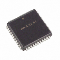
DS89C450-QNL+ Maxim Integrated Products, DS89C450-QNL+ Datasheet - Page 30

DS89C450-QNL+
Manufacturer Part Number
DS89C450-QNL+
Description
IC MCU FLASH 64KB 33MHZ 44-PLCC
Manufacturer
Maxim Integrated Products
Series
89Cr
Datasheet
1.DS89C450-KIT.pdf
(46 pages)
Specifications of DS89C450-QNL+
Core Processor
8051
Core Size
8-Bit
Speed
33MHz
Connectivity
EBI/EMI, SIO, UART/USART
Peripherals
Power-Fail Reset, WDT
Number Of I /o
32
Program Memory Size
64KB (64K x 8)
Program Memory Type
FLASH
Ram Size
1K x 8
Voltage - Supply (vcc/vdd)
4.5 V ~ 5.5 V
Oscillator Type
External
Operating Temperature
-40°C ~ 85°C
Package / Case
44-LCC, 44-PLCC
Processor Series
89C
Core
8051
Data Bus Width
8 bit
Data Ram Size
1 KB
Maximum Clock Frequency
33 MHz
Number Of Programmable I/os
32
Number Of Timers
3
Operating Supply Voltage
5 V
Maximum Operating Temperature
+ 85 C
Mounting Style
SMD/SMT
3rd Party Development Tools
PK51, CA51, A51, ULINK2
Development Tools By Supplier
DS89C450-K00
Minimum Operating Temperature
- 40 C
Interface Type
UART
Lead Free Status / RoHS Status
Lead free / RoHS Compliant
Eeprom Size
-
Data Converters
-
Lead Free Status / Rohs Status
Lead free / RoHS Compliant
Figure 10. Page Mode 1, External Memory Cycle (CD1:CD0 = 10)
During a page miss, P2 drives the Addr [8:15] of the 16-bit address and holds it for the duration of the first half of
the memory cycle to allow the external address latches to latch the new most significant address byte. ALE is
asserted to strobe the external address latches. During this operation, PSEN, RD, and WR are held in inactive
states and P0 is in a high-impedance state. The following half-memory cycle is executed as a page hit cycle and
the appropriate operation takes place.
A page miss can occur at set intervals or during external operations that require a memory access into a page of
memory that has not been accessed during the last external cycle. Generally, the first external memory access
causes a page miss. The new page address is stored internally and is used to detect a page miss for the current
external memory cycle.
Internal Memory Cycles
XTAL1
Port 0
Port 2
RD/WR
Port 0
Port 2
RD/WR
RD/WR
PSEN
Port 2
Port 0
ALE
PSEN
ALE
PSEN
ALE
MSB
Page Miss
MSBAdd
LSB
Page Miss
Inst
MSBAdd
LSB
Inst
Page Hit
LSB Add
LSB
MOVX
External Memory Cycles
Page Miss
MOVX MOVX
LSB
MOVX executed
DS89C430/DS89C450 Ultra-High-Speed Flash Microcontrollers
Page Hit
30 of 46
LSB Add
MSB
Data Access
Inst
MOVX executed
LSB Add
LSB
Data
MSBAdd
Inst
MSB
Page Miss
Data Access
MOVX executed
LSB
Inst
LSB Add
Data Access
MSB
Data
Data Access
LSB Add
LSB
next instruction
Data
MSBAdd
Page Miss
Data
MSB
PAGES=00
PAGES=01
PAGES=10


