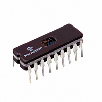
PIC16C54B/JW Microchip Technology, PIC16C54B/JW Datasheet - Page 64

PIC16C54B/JW
Manufacturer Part Number
PIC16C54B/JW
Description
MICRO CTRL 512 X 12 EPROM 18CDIP
Manufacturer
Microchip Technology
Series
PIC® 16Cr
Specifications of PIC16C54B/JW
Core Processor
PIC
Core Size
8-Bit
Speed
20MHz
Peripherals
POR, WDT
Number Of I /o
12
Program Memory Size
768B (512 x 12)
Program Memory Type
EPROM, UV
Ram Size
25 x 8
Voltage - Supply (vcc/vdd)
3 V ~ 5.5 V
Oscillator Type
External
Operating Temperature
0°C ~ 70°C
Package / Case
18-CDIP (0.300", 7.62mm) Window
Lead Free Status / RoHS Status
Contains lead / RoHS non-compliant
Eeprom Size
-
Data Converters
-
Connectivity
-
Available stocks
Company
Part Number
Manufacturer
Quantity
Price
- Current page: 64 of 218
- Download datasheet (2Mb)
PIC16C5X
FIGURE 10-3: CLKOUT AND I/O TIMING - PIC16C52
TABLE 10-2:
DS30453B-page 64
Note 1: Data in the Typical (“Typ”) column is at 5V, 25 C unless otherwise stated. These parameters are for design guidance only
*
** These parameters are design targets and are not tested. No characterization data available at this time.
Parameter
CLKOUT
I/O Pin
(output)
AC Characteristics
These parameters are characterized but not tested.
2: Measurements are taken in RC Mode where CLKOUT output is 4 x T
3: See Figure 10-1 for loading conditions.
I/O Pin
(input)
OSC1
No.
10
11
12
13
14
15
16
17
18
19
20
21
Note: All tests must be done with specified capacitive loads (see data sheet) 50 pF on I/O pins and CLKOUT.
and are not tested.
TosH2ckL
TosH2ckH
TckR
TckF
TckL2ioV
TioV2ckH
TckH2ioI
TosH2ioV
TosH2ioI
TioV2osH
TioR
TioF
CLKOUT AND I/O TIMING REQUIREMENTS - PIC16C52
Sym
Old Value
Q4
Standard Operating Conditions (unless otherwise specified)
Operating Temperature
Operating Voltage V
OSC1 to CLKOUT
OSC1 to CLKOUT
CLKOUT rise time
CLKOUT fall time
CLKOUT to Port out valid
Port in valid before CLKOUT
Port in hold after CLKOUT
OSC1 (Q1 cycle) to Port out valid
OSC1 (Q2 cycle) to Port input invalid
(I/O in hold time)
Port input valid to OSC1
(I/O in setup time)
Port output rise time
Port output fall time
10
13
Characteristic
17
14
(2)
20, 21
(2)
(3)
(3)
(2)
(2)
Preliminary
Q1
DD
range is described in Section 10.1.
(2)
(2)
(2)
–40 C
0 C
19
(3)
T
T
18
A
A
OSC
+70 C (commercial)
+85 C (industrial)
0.25 T
.
Q2
15
TBD
TBD
Min
—
—
—
—
—
—
—
—
0*
CY
+
30*
Typ
1998 Microchip Technology Inc.
15
15
10
10
—
—
—
—
—
—
5
5
11
(1)
12
New Value
16
100*
Q3
Max
30**
30**
15**
15**
40**
25**
25**
PIC16C52
—
—
—
—
Units
ns
ns
ns
ns
ns
ns
ns
ns
ns
ns
ns
ns
Related parts for PIC16C54B/JW
Image
Part Number
Description
Manufacturer
Datasheet
Request
R

Part Number:
Description:
IC MCU OTP 512X12 18SOIC
Manufacturer:
Microchip Technology
Datasheet:

Part Number:
Description:
IC MCU OTP 512X12 18DIP
Manufacturer:
Microchip Technology
Datasheet:

Part Number:
Description:
IC MCU OTP 512X12 18SOIC
Manufacturer:
Microchip Technology
Datasheet:

Part Number:
Description:
IC MCU OTP 512X12 18SOIC
Manufacturer:
Microchip Technology
Datasheet:

Part Number:
Description:
IC MCU OTP 512X12 18SOIC
Manufacturer:
Microchip Technology
Datasheet:

Part Number:
Description:
IC MCU OTP 512X12 18DIP
Manufacturer:
Microchip Technology
Datasheet:

Part Number:
Description:
IC MCU OTP 512X12 18DIP
Manufacturer:
Microchip Technology
Datasheet:

Part Number:
Description:
IC MCU OTP 512X12 18DIP
Manufacturer:
Microchip Technology
Datasheet:

Part Number:
Description:
IC MCU OTP 512X12 18SOIC
Manufacturer:
Microchip Technology
Datasheet:

Part Number:
Description:
IC MCU OTP 512X12 18DIP
Manufacturer:
Microchip Technology
Datasheet:

Part Number:
Description:
IC MCU OTP 512X12 18SOIC
Manufacturer:
Microchip Technology
Datasheet:

Part Number:
Description:
IC MCU OTP 512X12 18SOIC
Manufacturer:
Microchip Technology
Datasheet:

Part Number:
Description:
IC MCU OTP 512X12 18DIP
Manufacturer:
Microchip Technology
Datasheet:

Part Number:
Description:
IC MCU OTP 512X12 18SOIC
Manufacturer:
Microchip Technology
Datasheet:

Part Number:
Description:
IC, 8BIT MCU, PIC16C, 40MHZ, DIP-18
Manufacturer:
Microchip Technology
Datasheet:


