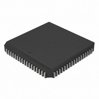
PIC17C762-33/L Microchip Technology, PIC17C762-33/L Datasheet - Page 203

PIC17C762-33/L
Manufacturer Part Number
PIC17C762-33/L
Description
IC MCU OTP 8KX16 A/D 84PLCC
Manufacturer
Microchip Technology
Series
PIC® 17Cr
Datasheets
1.PIC16F616T-ISL.pdf
(8 pages)
2.PIC17C752-16L.pdf
(304 pages)
3.PIC17C752-16L.pdf
(6 pages)
Specifications of PIC17C762-33/L
Core Size
8-Bit
Program Memory Size
16KB (8K x 16)
Peripherals
Brown-out Detect/Reset, POR, PWM, WDT
Core Processor
PIC
Speed
33MHz
Connectivity
I²C, SPI, UART/USART
Number Of I /o
66
Program Memory Type
OTP
Ram Size
678 x 8
Voltage - Supply (vcc/vdd)
4.5 V ~ 5.5 V
Data Converters
A/D 16x10b
Oscillator Type
External
Operating Temperature
0°C ~ 70°C
Package / Case
84-PLCC
Controller Family/series
PIC17
No. Of I/o's
66
Ram Memory Size
678Byte
Cpu Speed
33MHz
No. Of Timers
4
Processor Series
PIC17C
Core
PIC
Data Bus Width
8 bit
Data Ram Size
678 B
Interface Type
I2C, MSSP, RS- 232, SCI, SPI, USART
Maximum Clock Frequency
33 MHz
Number Of Programmable I/os
66
Number Of Timers
8
Operating Supply Voltage
3 V to 5.5 V
Maximum Operating Temperature
+ 70 C
Mounting Style
SMD/SMT
Development Tools By Supplier
ICE2000, DM173001
Minimum Operating Temperature
0 C
On-chip Adc
16 bit
Lead Free Status / RoHS Status
Lead free / RoHS Compliant
For Use With
AC164308 - MODULE SKT FOR PM3 68PLCCDVA17XL841 - DEVICE ADAPTER FOR PIC17C762DM173001 - KIT DEVELOPMENT PICDEM17AC164027 - ADAPTER PICSTART PLUS 84PLCCAC174012 - MODULE SKT PROMATEII 84PLCC
Eeprom Size
-
Lead Free Status / Rohs Status
Details
Available stocks
Company
Part Number
Manufacturer
Quantity
Price
Company:
Part Number:
PIC17C762-33/L
Manufacturer:
Microchip Technology
Quantity:
10 000
- Current page: 203 of 304
- Download datasheet (6Mb)
ADDWFC
Syntax:
Operands:
Operation:
Status Affected:
Encoding:
Description:
Words:
Cycles:
Q Cycle Activity:
Example:
2000 Microchip Technology Inc.
Before Instruction
After Instruction
Decode
Carry bit =
REG
WREG
Carry bit =
REG
WREG
Q1
=
=
=
=
register ’f’
ADD WREG and Carry bit to f
[ label ] ADDWFC
0
d
(WREG) + (f) + C
OV, C, DC, Z
Add WREG, the Carry Flag and data
memory location ’f’. If ’d’ is 0, the result is
placed in WREG. If ’d’ is 1, the result is
placed in data memory location ’f’.
1
1
ADDWFC
Read
Q2
0001
1
0x02
0x4D
0
0x02
0x50
f
[0,1]
255
000d
REG
Process
Data
Q3
0
ffff
(dest)
f,d
destination
Write to
Q4
ffff
ANDLW
Syntax:
Operands:
Operation:
Status Affected:
Encoding:
Description:
Words:
Cycles:
Q Cycle Activity:
Example:
Before Instruction
After Instruction
Decode
WREG
WREG
Q1
=
=
Read literal
And Literal with WREG
[ label ] ANDLW
0
(WREG) .AND. (k)
Z
The contents of WREG are AND’ed with
the 8-bit literal 'k'. The result is placed in
WREG.
1
1
ANDLW
1011
Q2
'k'
0xA3
0x03
k
PIC17C7XX
255
0101
0x5F
Process
Data
Q3
DS30289B-page 203
k
kkkk
(WREG)
Write to
WREG
Q4
kkkk
Related parts for PIC17C762-33/L
Image
Part Number
Description
Manufacturer
Datasheet
Request
R

Part Number:
Description:
IC MCU OTP 8KX16 A/D 80TQFP
Manufacturer:
Microchip Technology
Datasheet:

Part Number:
Description:
IC MCU OTP 8KX16 A/D 80TQFP
Manufacturer:
Microchip Technology
Datasheet:

Part Number:
Description:
IC MCU OTP 8KX16 A/D 84PLCC
Manufacturer:
Microchip Technology
Datasheet:

Part Number:
Description:
IC MCU OTP 8KX16 A/D 84PLCC
Manufacturer:
Microchip Technology
Datasheet:

Part Number:
Description:
IC MCU OTP 8KX16 A/D 84PLCC
Manufacturer:
Microchip Technology
Datasheet:

Part Number:
Description:
IC MCU OTP 8KX16 A/D 80TQFP
Manufacturer:
Microchip Technology
Datasheet:

Part Number:
Description:
IC MCU OTP 8KX16 A/D 80TQFP
Manufacturer:
Microchip Technology
Datasheet:

Part Number:
Description:
IC MCU CMOS 16MHZ 8K EPRM 84PLCC
Manufacturer:
Microchip Technology
Datasheet:

Part Number:
Description:
IC MCU CMOS 16MHZ 8K EPRM 80TQFP
Manufacturer:
Microchip Technology
Datasheet:

Part Number:
Description:
IC MCU CMOS 33MHZ 8K EPRM 84PLCC
Manufacturer:
Microchip Technology
Datasheet:

Part Number:
Description:
IC MCU CMOS 33MHZ 8K EPRM 80TQFP
Manufacturer:
Microchip Technology
Datasheet:

Part Number:
Description:
Manufacturer:
Microchip Technology Inc.
Datasheet:

Part Number:
Description:
Manufacturer:
Microchip Technology Inc.
Datasheet:


