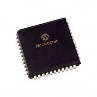
PIC16C662-10I/L Microchip Technology, PIC16C662-10I/L Datasheet - Page 39

PIC16C662-10I/L
Manufacturer Part Number
PIC16C662-10I/L
Description
IC MCU OTP 4KX14 COMP 44PLCC
Manufacturer
Microchip Technology
Series
PIC® 16Cr
Specifications of PIC16C662-10I/L
Core Processor
PIC
Core Size
8-Bit
Speed
10MHz
Peripherals
Brown-out Detect/Reset, LED, POR, WDT
Number Of I /o
33
Program Memory Size
7KB (4K x 14)
Program Memory Type
OTP
Ram Size
176 x 8
Voltage - Supply (vcc/vdd)
4 V ~ 6 V
Oscillator Type
External
Operating Temperature
-40°C ~ 85°C
Package / Case
44-PLCC
Processor Series
PIC16C
Core
PIC
Data Bus Width
8 bit
Data Ram Size
176 B
Interface Type
RS- 232
Maximum Clock Frequency
10 MHz
Number Of Programmable I/os
33
Number Of Timers
8
Operating Supply Voltage
3 V to 6 V
Maximum Operating Temperature
+ 85 C
Mounting Style
SMD/SMT
3rd Party Development Tools
52715-96, 52716-328, 52717-734
Development Tools By Supplier
ICE2000, DM163022
Minimum Operating Temperature
- 40 C
On-chip Adc
10 bit
For Use With
DVA16XL441 - ADAPTER DEVICE ICE 44PLCC309-1040 - ADAPTER 44-PLCC ZIF TO 40-DIP309-1039 - ADAPTER 44-PLCC TO 40-DIP
Lead Free Status / RoHS Status
Lead free / RoHS Compliant
Eeprom Size
-
Data Converters
-
Connectivity
-
Lead Free Status / Rohs Status
Details
Available stocks
Company
Part Number
Manufacturer
Quantity
Price
Company:
Part Number:
PIC16C662-10I/L
Manufacturer:
Microchip Technology
Quantity:
10 000
5.7
PORTD operates as an 8-bit wide parallel slave port, or
as a microprocessor port when control bit PSPMODE
(TRISE<4>) is set. In slave mode it is asynchronously
readable and writable by the external world through
RD control input pin (RE0/RD) and WR control input pin
(RE1/WR).
It can directly interface to an 8-bit microprocessor data
bus. The external microprocessor can read or write the
PORTD latch as an 8-bit latch. Setting PSPMODE
enables port pin RE0/RD to be the RD input, RE1/WR
to be the WR input and RE2/CS to be the CS (chip
select) input. For this functionality, the corresponding
data direction bits of the TRISE register (TRISE<2:0>)
must be configured as inputs (set).
There are actually two 8-bit latches, one for data-out
(from the PIC16/17) and one for data input. The user
writes 8-bit data to PORTD data latch and reads data
from the port pin latch (note that they have the same
address). In this mode, the TRISD register is ignored
since the microprocessor is controlling the direction of
data flow.
Input Buffer Full Status Flag bit IBF (TRISE<7>) is set
if a received word is waiting to be read by the CPU.
Once the PORTD input latch is read, bit IBF is cleared.
IBF is a read only status bit. Output Buffer Full Status
Flag bit OBF (TRISE<6>) is set if a word written to
PORTD latch is waiting to be read by the external bus.
Once the PORTD output latch is read by the micropro-
cessor, bit OBF is cleared. Input Buffer Overflow Status
flag bit IBOV (TRISE<5>) is set if a second write to the
microprocessor port is attempted when the previous
word has not been read by the CPU (the first word is
retained in the buffer).
When not in Parallel Slave Port mode, bits IBF and
OBF are held clear. However, if flag bit IBOV was pre-
viously set, it must be cleared in software.
TABLE 5-11:
Address Name
08h
09h
89h
0Ch
8Ch
Legend: x = unknown, u = unchanged, - = unimplemented locations read as '0'. Shaded cells are not used by the PSP.
Note 1: These bits are reserved on the PIC16C641/642, always maintain these bits clear.
1996 Microchip Technology Inc.
Parallel Slave Port
(PIC16C661 and PIC16C662 only)
PORTD
PORTE
TRISE
PIR1
PIE1
REGISTERS ASSOCIATED WITH PARALLEL SLAVE PORT
PSPIE
PSPIF
PSP7
Bit 7
IBF
—
(1)
(1)
PSP6 PSP5
CMIF
CMIE
Bit 6
OBF
—
IBOV
Bit 5
—
—
—
PSPMODE
PSP4
Bit 4
—
—
—
Preliminary
PIC16C64X & PIC16C66X
PSP3
Bit 3
—
—
—
—
An interrupt is generated and latched into flag bit
PSPIF (PIR1<7>) when a read or a write operation is
completed. Flag bit PSPIF must be cleared by user
software. The interrupt can be disabled by clearing the
interrupt enable bit PSPIE (PIE1<7>).
FIGURE 5-12: PORTD AND PORTE AS A
TRISE2 TRISE1 TRISE0
PSP2
One bit of PORTD
Bit 2
RE2
—
—
Data bus
Set interrupt flag
PSPIF (PIR1<7>)
Note: I/O pins have protection diodes to V
WR
PORT
RD
PORT
PSP1
Bit 1
RE1
—
—
Q
D
CK
PARALLEL SLAVE PORT
EN
PSP0
Bit 0
RE0
EN
Q
—
—
D
xxxx xxxx
---- -xxx
0000 -111
00-- ----
00-- ----
Value on:
Chip Select
POR,
BOR
Read
Write
DS30559A-page 39
TTL
TTL
TTL
TTL
other resets
DD
Value on all
uuuu uuuu
---- -uuu
0000 -111
00-- ----
00-- ----
and V
CS
WR
RD
RDx
pin
SS
.


