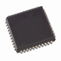
AT89C55WD-24JI Atmel, AT89C55WD-24JI Datasheet - Page 20

AT89C55WD-24JI
Manufacturer Part Number
AT89C55WD-24JI
Description
IC MICRO CTRL 24MHZ 44PLCC
Manufacturer
Atmel
Series
89Cr
Datasheet
1.AT89C55WD-24AU.pdf
(35 pages)
Specifications of AT89C55WD-24JI
Core Processor
8051
Core Size
8-Bit
Speed
24MHz
Connectivity
UART/USART
Peripherals
WDT
Number Of I /o
32
Program Memory Size
20KB (20K x 8)
Program Memory Type
FLASH
Ram Size
256 x 8
Voltage - Supply (vcc/vdd)
4.5 V ~ 5.5 V
Oscillator Type
Internal
Operating Temperature
-40°C ~ 85°C
Package / Case
44-PLCC
Lead Free Status / RoHS Status
Contains lead / RoHS non-compliant
Eeprom Size
-
Data Converters
-
Other names
AT89C55WD24JI
Available stocks
Company
Part Number
Manufacturer
Quantity
Price
Company:
Part Number:
AT89C55WD-24JI
Manufacturer:
AGILENT
Quantity:
650
Company:
Part Number:
AT89C55WD-24JI
Manufacturer:
ATM
Quantity:
2 430
Company:
Part Number:
AT89C55WD-24JI
Manufacturer:
ATM
Quantity:
2 430
Company:
Part Number:
AT89C55WD-24JI
Manufacturer:
ATMEL
Quantity:
3
Part Number:
AT89C55WD-24JI
Manufacturer:
ATMEL/爱特梅尔
Quantity:
20 000
19. Program Memory Lock Bits
20. Programming the Flash
20
AT89C55WD
The AT89C55WD has three lock bits that can be left unprogrammed (U) or can be programmed
(P) to obtain the additional features listed in the following table.
Table 19-1.
When lock bit 1 is programmed, the logic level at the EA pin is sampled and latched during reset.
If the device is powered up without a reset, the latch initializes to a random value and holds that
value until reset is activated. The latched value of EA must agree with the current logic level at
that pin in order for the device to function properly.
The AT89C55WD is shipped with the on-chip Flash memory array ready to be programmed. The
programming interface needs a high-voltage (12-volt) program enable signal and is compatible
with conventional third-party Flash or EPROM programmers.
The AT89C55WD code memory array is programmed byte-by-byte.
Programming Algorithm: Before programming the AT89C55WD, the address, data, and con-
trol signals should be set up according to the Flash programming mode table and Figures 21-1
and 21-2. To program the AT89C55WD, take the following steps:
1. Input the desired memory location on the address lines.
2. Input the appropriate data byte on the data lines.
3. Activate the correct combination of control signals.
4. Raise EA/V
5. Pulse ALE/PROG once to program a byte in the Flash array or the lock bits. The byte-
1
2
3
4
Program Lock Bits
write cycle is self-timed and typically takes no more than 50 µs. Repeat steps 1
through 5, changing the address and data for the entire array or until the end of the
object file is reached.
LB1
U
P
P
P
Lock Bit Protection Modes
LB2
PP
U
U
P
P
to 12V.
LB3
U
U
U
P
Protection Type
No program lock features.
MOVC instructions executed from external program memory are
disabled from fetching code bytes from internal memory, EA is
sampled and latched on reset, and further programming of the Flash
memory is disabled.
Same as mode 2, but verify is also disabled.
Same as mode 3, but external execution is also disabled.
1921D–MICRO–6/08


