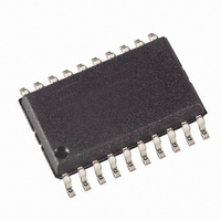
ATTINY26-16SI Atmel, ATTINY26-16SI Datasheet - Page 42

ATTINY26-16SI
Manufacturer Part Number
ATTINY26-16SI
Description
IC AVR MCU 2K 16MHZ IND 20-SOIC
Manufacturer
Atmel
Series
AVR® ATtinyr
Specifications of ATTINY26-16SI
Core Processor
AVR
Core Size
8-Bit
Speed
16MHz
Connectivity
USI
Peripherals
Brown-out Detect/Reset, POR, PWM, WDT
Number Of I /o
16
Program Memory Size
2KB (1K x 16)
Program Memory Type
FLASH
Eeprom Size
128 x 8
Ram Size
128 x 8
Voltage - Supply (vcc/vdd)
4.5 V ~ 5.5 V
Data Converters
A/D 11x10b
Oscillator Type
Internal
Operating Temperature
-40°C ~ 85°C
Package / Case
20-SOIC (7.5mm Width)
Lead Free Status / RoHS Status
Contains lead / RoHS non-compliant
Available stocks
Company
Part Number
Manufacturer
Quantity
Price
Part Number:
ATTINY26-16SI
Manufacturer:
ATMEL/爱特梅尔
Quantity:
20 000
- Current page: 42 of 182
- Download datasheet (3Mb)
Configuring the Pin
42
ATtiny26(L)
Figure 32. General Digital I/O
Note:
Each port pin consists of 3 Register bits: DDxn, PORTxn, and PINxn. As shown in “Register
Description for I/O Ports” on page 56, the DDxn bits are accessed at the DDRx I/O address, the
PORTxn bits at the PORTx I/O address, and the PINxn bits at the PINx I/O address.
The DDxn bit in the DDRx Register selects the direction of this pin. If DDxn is written logic one,
Pxn is configured as an output pin. If DDxn is written logic zero, Pxn is configured as an input
pin.
If PORTxn is written logic one when the pin is configured as an input pin, the pull-up resistor is
activated. To switch the pull-up resistor off, PORTxn has to be written logic zero or the pin has to
be configured as an output pin. The port pins are tri-stated when a reset condition becomes
active, even if no clocks are running.
If PORTxn is written logic one when the pin is configured as an output pin, the port pin is driven
high (one). If PORTxn is written logic zero when the pin is configured as an output pin, the port
pin is driven low (zero).
When switching between tri-state ({DDxn, PORTxn} = 0b00) and output high ({DDxn, PORTxn}
= 0b11), an intermediate state with either pull-up enabled ({DDxn, PORTxn} = 0b01) or output
low ({DDxn, PORTxn} = 0b10) must occur. Normally, the pull-up enabled state is fully
acceptable, as a high-impedant environment will not notice the difference between a strong high
driver and a pull-up. If this is not the case, the PUD bit in the MCUCR Register can be set to
disable all pull-ups in all ports.
Switching between input with pull-up and output low generates the same problem. The user
must use either the tri-state ({DDxn, PORTxn} = 0b00) or the output high state ({DDxn, PORTxn}
= 0b11) as an intermediate step.
1. WPx, WDx, RRx, RPx, and RDx are common to all pins within the same port. clk
Pxn
and PUD are common to all ports.
PUD:
SLEEP:
clk
I/O
:
PULLUP DISABLE
SLEEP CONTROL
I/O CLOCK
(1)
SLEEP
SYNCHRONIZER
WDx:
RDx:
WPx:
RRx:
RPx:
D
L
Q
Q
D
PINxn
WRITE DDRx
READ DDRx
WRITE PORTx
READ PORTx REGISTER
READ PORTx PIN
Q
Q
RESET
RESET
PORTxn
Q
Q
Q
Q
DDxn
CLR
CLR
D
D
PUD
WDx
RDx
WPx
RRx
RPx
clk
I/O
1477K–AVR–08/10
I/O
, SLEEP,
Related parts for ATTINY26-16SI
Image
Part Number
Description
Manufacturer
Datasheet
Request
R

Part Number:
Description:
Manufacturer:
Atmel Corporation
Datasheet:

Part Number:
Description:
IC AVR MCU 2K 16MHZ IND 32-QFN
Manufacturer:
Atmel
Datasheet:

Part Number:
Description:
IC AVR MCU 2K 16MHZ IND 20-SOIC
Manufacturer:
Atmel
Datasheet:

Part Number:
Description:
IC AVR MCU 2K 16MHZ IND 20-DIP
Manufacturer:
Atmel
Datasheet:

Part Number:
Description:
IC AVR MCU 2K 16MHZ IND 32-QFN
Manufacturer:
Atmel
Datasheet:

Part Number:
Description:
IC AVR MCU 2K 16MHZ IND 20-DIP
Manufacturer:
Atmel
Datasheet:

Part Number:
Description:
IC AVR MCU 2K 16MHZ COM 20-SOIC
Manufacturer:
Atmel
Datasheet:

Part Number:
Description:
ID MCU AVR 2K 5V 16MHZ 32-QFN
Manufacturer:
Atmel
Datasheet:

Part Number:
Description:
Microcontrollers (MCU) AVR 2K FLASH 128B EE 128B SRAM ADC
Manufacturer:
Atmel
Datasheet:

Part Number:
Description:
IC AVR MCU 2K 16MHZ COM 32-QFN
Manufacturer:
Atmel
Datasheet:

Part Number:
Description:
IC AVR MCU 2K 16MHZ COM 20-DIP
Manufacturer:
Atmel
Datasheet:

Part Number:
Description:
ID MCU AVR 2K 5V 16MHZ 20-DIP
Manufacturer:
Atmel
Datasheet:

Part Number:
Description:
ID MCU AVR 2K 5V 16MHZ 20-SOIC
Manufacturer:
Atmel
Datasheet:

Part Number:
Description:
IC MCU AVR 2K 16MHZ IND 20SOIC
Manufacturer:
Atmel
Datasheet:


