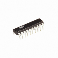
ATTINY2313-20PJ Atmel, ATTINY2313-20PJ Datasheet - Page 5

ATTINY2313-20PJ
Manufacturer Part Number
ATTINY2313-20PJ
Description
IC MCU AVR 2K FLASH 20DIP
Manufacturer
Atmel
Series
AVR® ATtinyr
Specifications of ATTINY2313-20PJ
Core Processor
AVR
Core Size
8-Bit
Speed
20MHz
Connectivity
SPI, UART/USART
Peripherals
Brown-out Detect/Reset, POR, PWM, WDT
Number Of I /o
18
Program Memory Size
2KB (1K x 16)
Program Memory Type
FLASH
Eeprom Size
128 x 8
Ram Size
128 x 8
Voltage - Supply (vcc/vdd)
2.7 V ~ 5.5 V
Oscillator Type
Internal
Operating Temperature
-40°C ~ 85°C
Package / Case
20-DIP (0.300", 7.62mm)
Lead Free Status / RoHS Status
Lead free / RoHS Compliant
Data Converters
-
Other names
ATTINY2313-24PJ
ATTINY2313-24PJ
ATTINY2313-24PJ
Pin Descriptions
VCC
GND
Port A (PA2..PA0)
Port B (PB7..PB0)
Port D (PD6..PD0)
RESET
XTAL1
XTAL2
2543ES–AVR–04/04
Digital supply voltage.
Ground.
Port A is a 3-bit bi-directional I/O port with internal pull-up resistors (selected for each
bit). The Port A output buffers have symmetrical drive characteristics with both high sink
and source capability. As inputs, Port A pins that are externally pulled low will source
current if the pull-up resistors are activated. The Port A pins are tri-stated when a reset
condition becomes active, even if the clock is not running.
Port A also serves the functions of various special features of the ATtiny2313 as listed
on page 52.
Port B is an 8-bit bi-directional I/O port with internal pull-up resistors (selected for each
bit). The Port B output buffers have symmetrical drive characteristics with both high sink
and source capability. As inputs, Port B pins that are externally pulled low will source
current if the pull-up resistors are activated. The Port B pins are tri-stated when a reset
condition becomes active, even if the clock is not running.
Port B also serves the functions of various special features of the ATtiny2313 as listed
on page 52.
Port D is a 7-bit bi-directional I/O port with internal pull-up resistors (selected for each
bit). The Port D output buffers have symmetrical drive characteristics with both high sink
and source capability. As inputs, Port D pins that are externally pulled low will source
current if the pull-up resistors are activated. The Port D pins are tri-stated when a reset
condition becomes active, even if the clock is not running.
Port D also serves the functions of various special features of the ATtiny2313 as listed
on page 55.
Reset input. A low level on this pin for longer than the minimum pulse length will gener-
ate a reset, even if the clock is not running. The minimum pulse length is given in Table
15 on page 33. Shorter pulses are not guaranteed to generate a reset. The Reset Input
is an alternate function for PA2 and dW.
Input to the inverting Oscillator amplifier and input to the internal clock operating circuit.
XTAL1 is an alternate function for PA0.
Output from the inverting Oscillator amplifier. XTAL2 is an alternate function for PA1.
ATtiny2313/V
5


