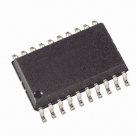
ATTINY167-15SZ Atmel, ATTINY167-15SZ Datasheet - Page 81

ATTINY167-15SZ
Manufacturer Part Number
ATTINY167-15SZ
Description
MCU AVR 16K FLASH 15MHZ 20-SOIC
Manufacturer
Atmel
Series
AVR® ATtinyr
Datasheet
1.ATTINY167-15MD.pdf
(283 pages)
Specifications of ATTINY167-15SZ
Core Processor
AVR
Core Size
8-Bit
Speed
16MHz
Connectivity
I²C, LIN, SPI, UART/USART, USI
Peripherals
Brown-out Detect/Reset, POR, PWM, Temp Sensor, WDT
Number Of I /o
16
Program Memory Size
16KB (8K x 16)
Program Memory Type
FLASH
Eeprom Size
512 x 8
Ram Size
512 x 8
Voltage - Supply (vcc/vdd)
2.7 V ~ 5.5 V
Data Converters
A/D 11x10b
Oscillator Type
Internal
Operating Temperature
-40°C ~ 125°C
Package / Case
20-SOIC (7.5mm Width)
For Use With
ATSTK600-SOIC - STK600 SOCKET/ADAPTER FOR SOIC
Lead Free Status / RoHS Status
Lead free / RoHS Compliant
- Current page: 81 of 283
- Download datasheet (5Mb)
9.3.4
7728G–AVR–06/10
Alternate Functions of Port B
The Port B pins with alternate functions are shown in
Table 9-6.
The alternate pin configuration is as follows:
• PCINT15/ADC10/OC1BX/RESET/dW – Port B, Bit 7
PCINT15: Pin Change Interrupt, source 15.
ADC10: Analog to Digital Converter, channel 10.
OC1BX: Output Compare and PWM Output B-X for Timer/Counter1. The PB7 pin has to be
Port Pin
PB7
PB6
PB5
PB4
PB3
PB2
PB1
PB0
configured as an output (DDB7 set (one)) to serve this function. The OC1BX pin is
also the output pin for the PWM mode timer function (c.f. OC1BX bit of TCCR1D regis-
ter).
Port B Pins Alternate Functions
Alternate Functions
PCINT15 (Pin Change Interrupt 15)
ADC10 (ADC Input Channel 10)
OC1BX (Output Compare and PWM Output B-X for Timer/Counter1)
RESET (Reset input pin)
dW (
PCINT14 (Pin Change Interrupt 14)
ADC9 (ADC Input Channel 9)
OC1AX (Output Compare and PWM Output A-X for Timer/Counter1)
INT0 (External Interrupt0 Input)
PCINT13 (Pin Change Interrupt 13)
ADC8 (ADC Input Channel 8)
OC1BW (Output Compare and PWM Output B-W for Timer/Counter1)
XTAL2 (Chip clock Oscillator pin 2)
CLKO (System clock output)
PCINT12 (Pin Change Interrupt 12)
OC1AW (Output Compare and PWM Output A-W for Timer/Counter1)
XTAL1 (Chip clock Oscillator pin 1)
CLKI (External clock input)
PCINT11 (Pin Change Interrupt 11)
OC1BV (Output Compare and PWM Output B-V for Timer/Counter1)
PCINT10 (Pin Change Interrupt 10)
OC1AV (Output Compare and PWM Output A-V for Timer/Counter1)
USCK (Three-wire Mode USI Default Clock Input)
SCL (Two-wire Mode USI Default Clock Input)
PCINT9 (Pin Change Interrupt 9)
OC1BU (Output Compare and PWM Output B-U for Timer/Counter1)
DO (Three-wire Mode USI Default Data Output)
PCINT8 (Pin Change Interrupt 8)
OC1AU (Output Compare and PWM Output A-U for Timer/Counter1)
DI (Three-wire Mode USI Default Data Input)
SDA (Two-wire Mode USI Default Data Input / Output)
debugWIRE
I/O)
Table
ATtiny87/ATtiny167
9-6.
81
Related parts for ATTINY167-15SZ
Image
Part Number
Description
Manufacturer
Datasheet
Request
R

Part Number:
Description:
Manufacturer:
Atmel Corporation
Datasheet:

Part Number:
Description:
Manufacturer:
Atmel Corporation
Datasheet:

Part Number:
Description:
MCU AVR 16K FLASH 15MHZ 32-QFN
Manufacturer:
Atmel
Datasheet:

Part Number:
Description:
IC MCU AVR 16K FLASH 20TSSOP
Manufacturer:
Atmel
Datasheet:

Part Number:
Description:
MCU AVR 16K FLASH 15MHZ 32-QFN
Manufacturer:
Atmel
Datasheet:

Part Number:
Description:
MCU AVR 16K FLASH 15MHZ 20-TSSOP
Manufacturer:
Atmel
Datasheet:

Part Number:
Description:
MCU AVR 16K FLASH 15MHZ 20-TSSOP
Manufacturer:
Atmel
Datasheet:

Part Number:
Description:
IC MCU AVR 16K FLASH 20SOIC
Manufacturer:
Atmel
Datasheet:


