C8051F311 Silicon Laboratories Inc, C8051F311 Datasheet - Page 39
C8051F311
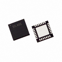
Manufacturer Part Number
C8051F311
Description
IC 8051 MCU 16K FLASH 28MLP
Manufacturer
Silicon Laboratories Inc
Series
C8051F31xr
Specifications of C8051F311
Core Processor
8051
Core Size
8-Bit
Speed
25MHz
Connectivity
SMBus (2-Wire/I²C), SPI, UART/USART
Peripherals
POR, PWM, Temp Sensor, WDT
Number Of I /o
25
Program Memory Size
16KB (16K x 8)
Program Memory Type
FLASH
Ram Size
1.25K x 8
Voltage - Supply (vcc/vdd)
2.7 V ~ 3.6 V
Data Converters
A/D 17x10b
Oscillator Type
Internal
Operating Temperature
-40°C ~ 85°C
Package / Case
28-VQFN Exposed Pad, 28-HVQFN, 28-SQFN, 28-DHVQFN
Lead Free Status / RoHS Status
Contains lead / RoHS non-compliant
Eeprom Size
-
Available stocks
Company
Part Number
Manufacturer
Quantity
Price

Part Number:
C8051F311-GM
Manufacturer:
SILICONLABS/èٹ¯ç§‘
Quantity:
20 000
Part Number:
C8051F311-GMR
Manufacturer:
SILICON LABS/èٹ¯ç§‘
Quantity:
20 000


4.
CNVSTR
XTAL1
XTAL2
Name
C2CK
VREF
GND
RST/
P3.0/
P0.0/
P0.2/
P0.3/
P0.6/
C2D
P0.1
P0.4
P0.5
P0.7
P1.0
P1.1
P1.2
P1.3
P1.4
V
DD
Pinout and Package Definitions
‘F310/2/4 ‘F311/3/5 ‘F316/7
32
31
30
29
28
27
26
25
24
23
22
4
3
5
6
2
1
Pin Numbers
Table 4.1. Pin Definitions for the C8051F31x
28
27
26
25
24
23
22
21
20
19
18
4
3
5
6
2
1
24
23
22
21
20
19
18
17
16
15
14
4
3
5
6
2
1
A Out or
D I/O or
D I/O or
D I/O or
D I/O or
D I/O or
D I/O
D I/O
D I/O
D I/O
D I/O
D I/O
D I/O
D I/O
D I/O
D I/O
D I/O
Type
D In
A In
A In
A In
A In
A In
A In
A In
Rev. 1.7
Description
Power Supply Voltage.
Ground.
Device Reset. Open-drain output of internal POR. An
external source can initiate a system reset by driving
this pin low for at least 10 µs.
Clock signal for the C2 Debug Interface.
Port 3.0. See
Bi-directional data signal for the C2 Debug Interface.
Port 0.0. See
External VREF input. (‘F310/1/2/3 only)
Port 0.1. See
Port 0.2. See
External Clock Input. This pin is the external oscillator
return for a crystal or resonator.
Port 0.3. See
External Clock Output. For an external crystal or reso-
nator, this pin is the excitation driver. This pin is the
external clock input for CMOS, capacitor, or RC oscil-
lator configurations.
Port 0.4. See
Port 0.5. See
Port 0.6. See
ADC0 External Convert Start Input. (‘F310/1/2/3 only)
Port 0.7. See
Port 1.0. See
Port 1.1. See
Port 1.2. See
Port 1.3. See
Port 1.4. See
C8051F310/1/2/3/4/5/6/7
Section 13
Section 13
Section 13
Section 13
Section 13
Section 13
Section 13
Section 13
Section 13
Section 13
Section 13
Section 13
Section 13
Section 13
for a complete description.
for a complete description.
for a complete description.
for a complete description.
for a complete description.
for a complete description.
for a complete description.
for a complete description.
for a complete description.
for a complete description.
for a complete description.
for a complete description.
for a complete description.
for a complete description.
39
Related parts for C8051F311
Image
Part Number
Description
Manufacturer
Datasheet
Request
R

Part Number:
Description:
SMD/C°/SINGLE-ENDED OUTPUT SILICON OSCILLATOR
Manufacturer:
Silicon Laboratories Inc
Part Number:
Description:
Manufacturer:
Silicon Laboratories Inc
Datasheet:
Part Number:
Description:
N/A N/A/SI4010 AES KEYFOB DEMO WITH LCD RX
Manufacturer:
Silicon Laboratories Inc
Datasheet:
Part Number:
Description:
N/A N/A/SI4010 SIMPLIFIED KEY FOB DEMO WITH LED RX
Manufacturer:
Silicon Laboratories Inc
Datasheet:
Part Number:
Description:
N/A/-40 TO 85 OC/EZLINK MODULE; F930/4432 HIGH BAND (REV E/B1)
Manufacturer:
Silicon Laboratories Inc
Part Number:
Description:
EZLink Module; F930/4432 Low Band (rev e/B1)
Manufacturer:
Silicon Laboratories Inc
Part Number:
Description:
I°/4460 10 DBM RADIO TEST CARD 434 MHZ
Manufacturer:
Silicon Laboratories Inc
Part Number:
Description:
I°/4461 14 DBM RADIO TEST CARD 868 MHZ
Manufacturer:
Silicon Laboratories Inc
Part Number:
Description:
I°/4463 20 DBM RFSWITCH RADIO TEST CARD 460 MHZ
Manufacturer:
Silicon Laboratories Inc
Part Number:
Description:
I°/4463 20 DBM RADIO TEST CARD 868 MHZ
Manufacturer:
Silicon Laboratories Inc
Part Number:
Description:
I°/4463 27 DBM RADIO TEST CARD 868 MHZ
Manufacturer:
Silicon Laboratories Inc
Part Number:
Description:
I°/4463 SKYWORKS 30 DBM RADIO TEST CARD 915 MHZ
Manufacturer:
Silicon Laboratories Inc
Part Number:
Description:
N/A N/A/-40 TO 85 OC/4463 RFMD 30 DBM RADIO TEST CARD 915 MHZ
Manufacturer:
Silicon Laboratories Inc
Part Number:
Description:
I°/4463 20 DBM RADIO TEST CARD 169 MHZ
Manufacturer:
Silicon Laboratories Inc