C8051F353 Silicon Laboratories Inc, C8051F353 Datasheet - Page 10
C8051F353
Manufacturer Part Number
C8051F353
Description
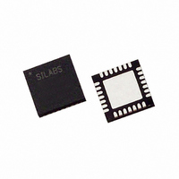
IC 8051 MCU 8K FLASH 28MLP
Manufacturer
Silicon Laboratories Inc
Series
C8051F35xr
Specifications of C8051F353
Core Processor
8051
Core Size
8-Bit
Speed
50MHz
Connectivity
SMBus (2-Wire/I²C), SPI, UART/USART
Peripherals
POR, PWM, Temp Sensor, WDT
Number Of I /o
17
Program Memory Size
8KB (8K x 8)
Program Memory Type
FLASH
Ram Size
768 x 8
Voltage - Supply (vcc/vdd)
2.7 V ~ 3.6 V
Data Converters
A/D 8x16b; D/A 2x8b
Oscillator Type
Internal
Operating Temperature
-40°C ~ 85°C
Package / Case
28-VQFN Exposed Pad, 28-HVQFN, 28-SQFN, 28-DHVQFN
Lead Free Status / RoHS Status
Contains lead / RoHS non-compliant
Eeprom Size
-
Available stocks
Company
Part Number
Manufacturer
Quantity
Price
Company:

Part Number:
C8051F353-GM
Manufacturer:
SiliconL
Quantity:
8 050


C8051F350/1/2/3
19. SMBus .................................................................................................................. 147
20. UART0 ................................................................................................................... 167
10
Figure 18.3. Crossbar Priority Decoder with No Pins Skipped ............................... 135
Figure 18.4. Crossbar Priority Decoder with Crystal Pins Skipped ........................ 136
Figure 18.5. XBR0: Port I/O Crossbar Register 0................................................... 138
Figure 18.6. XBR1: Port I/O Crossbar Register 1................................................... 139
Figure 18.7. P0: Port0 Register .............................................................................. 141
Figure 18.8. P0MDIN: Port0 Input Mode Register.................................................. 141
Figure 18.9. P0MDOUT: Port0 Output Mode Register ........................................... 142
Figure 18.10. P0SKIP: Port0 Skip Register............................................................ 142
Figure 18.11. P1: Port1 Register ............................................................................ 143
Figure 18.12. P1MDIN: Port1 Input Mode Register................................................ 143
Figure 18.13. P1MDOUT: Port1 Output Mode Register ......................................... 144
Figure 18.14. P1SKIP: Port1 Skip Register............................................................ 144
Figure 18.15. P2: Port2 Register ............................................................................ 145
Figure 18.16. P2MDOUT: Port2 Output Mode Register ......................................... 145
Table 18.1. Port I/O DC Electrical Characteristics.................................................. 146
Figure 19.1. SMBus Block Diagram ....................................................................... 147
Figure 19.2. Typical SMBus Configuration ............................................................. 148
Figure 19.3. SMBus Transaction ............................................................................ 149
Table 19.1. SMBus Clock Source Selection........................................................... 152
Figure 19.4. Typical SMBus SCL Generation......................................................... 153
Table 19.2. Minimum SDA Setup and Hold Times ................................................. 153
Figure 19.5. SMB0CF: SMBus Clock/Configuration Register ................................ 154
Figure 19.6. SMB0CN: SMBus Control Register.................................................... 156
Table 19.3. Sources for Hardware Changes to SMB0CN ...................................... 157
Figure 19.7. SMB0DAT: SMBus Data Register...................................................... 158
Figure 19.8. Typical Master Transmitter Sequence................................................ 159
Figure 19.9. Typical Master Receiver Sequence.................................................... 160
Figure 19.10. Typical Slave Receiver Sequence.................................................... 161
Figure 19.11. Typical Slave Transmitter Sequence................................................ 162
Table 19.4. SMBus Status Decoding...................................................................... 163
Figure 20.1. UART0 Block Diagram ....................................................................... 167
Figure 20.2. UART0 Baud Rate Logic .................................................................... 168
Figure 20.3. UART Interconnect Diagram .............................................................. 169
Figure 20.4. 8-Bit UART Timing Diagram............................................................... 169
Figure 20.5. 9-Bit UART Timing Diagram............................................................... 170
Figure 20.6. UART Multi-Processor Mode Interconnect Diagram .......................... 171
Figure 20.7. SCON0: Serial Port 0 Control Register .............................................. 172
Figure 20.8. SBUF0: Serial (UART0) Port Data Buffer Register ............................ 173
Table 20.1. Timer Settings for Standard Baud Rates Using the Internal Oscillator 174
Table 20.2. Timer Settings for Standard Baud Rates Using an External Oscillator 174
Table 20.3. Timer Settings for Standard Baud Rates Using an External Oscillator 175
Table 20.4. Timer Settings for Standard Baud Rates Using an External Oscillator 175
Table 20.5. Timer Settings for Standard Baud Rates Using an External Oscillator 176
Rev. 0.4
Related parts for C8051F353
Image
Part Number
Description
Manufacturer
Datasheet
Request
R

Part Number:
Description:
SMD/C°/SINGLE-ENDED OUTPUT SILICON OSCILLATOR
Manufacturer:
Silicon Laboratories Inc
Part Number:
Description:
Manufacturer:
Silicon Laboratories Inc
Datasheet:
Part Number:
Description:
N/A N/A/SI4010 AES KEYFOB DEMO WITH LCD RX
Manufacturer:
Silicon Laboratories Inc
Datasheet:
Part Number:
Description:
N/A N/A/SI4010 SIMPLIFIED KEY FOB DEMO WITH LED RX
Manufacturer:
Silicon Laboratories Inc
Datasheet:
Part Number:
Description:
N/A/-40 TO 85 OC/EZLINK MODULE; F930/4432 HIGH BAND (REV E/B1)
Manufacturer:
Silicon Laboratories Inc
Part Number:
Description:
EZLink Module; F930/4432 Low Band (rev e/B1)
Manufacturer:
Silicon Laboratories Inc
Part Number:
Description:
I°/4460 10 DBM RADIO TEST CARD 434 MHZ
Manufacturer:
Silicon Laboratories Inc
Part Number:
Description:
I°/4461 14 DBM RADIO TEST CARD 868 MHZ
Manufacturer:
Silicon Laboratories Inc
Part Number:
Description:
I°/4463 20 DBM RFSWITCH RADIO TEST CARD 460 MHZ
Manufacturer:
Silicon Laboratories Inc
Part Number:
Description:
I°/4463 20 DBM RADIO TEST CARD 868 MHZ
Manufacturer:
Silicon Laboratories Inc
Part Number:
Description:
I°/4463 27 DBM RADIO TEST CARD 868 MHZ
Manufacturer:
Silicon Laboratories Inc
Part Number:
Description:
I°/4463 SKYWORKS 30 DBM RADIO TEST CARD 915 MHZ
Manufacturer:
Silicon Laboratories Inc
Part Number:
Description:
N/A N/A/-40 TO 85 OC/4463 RFMD 30 DBM RADIO TEST CARD 915 MHZ
Manufacturer:
Silicon Laboratories Inc
Part Number:
Description:
I°/4463 20 DBM RADIO TEST CARD 169 MHZ
Manufacturer:
Silicon Laboratories Inc