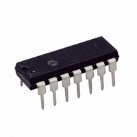
MCP6S26-I/P Microchip Technology, MCP6S26-I/P Datasheet - Page 9

MCP6S26-I/P
Manufacturer Part Number
MCP6S26-I/P
Description
IC PGA 6CH R-R I/O 14DIP
Manufacturer
Microchip Technology
Datasheet
1.MCP6S22DM-PICTL.pdf
(43 pages)
Specifications of MCP6S26-I/P
Amplifier Type
Programmable Gain
Number Of Circuits
6
Output Type
Push-Pull, Rail-to-Rail
Slew Rate
22 V/µs
-3db Bandwidth
12MHz
Current - Input Bias
1pA
Voltage - Input Offset
275µV
Current - Supply
1mA
Current - Output / Channel
30mA
Voltage - Supply, Single/dual (±)
2.5 V ~ 5.5 V
Operating Temperature
-40°C ~ 85°C
Mounting Type
Through Hole
Package / Case
14-DIP (0.300", 7.62mm)
No. Of Amplifiers
1
Bandwidth
12MHz
Rail To Rail I/o Type
Rail Rail I/O
No. Of Channels
6
Supply Voltage Range
2.5V To 5.5V
Amplifier Case Style
DIP
No. Of Pins
14
Lead Free Status / RoHS Status
Lead free / RoHS Compliant
Gain Bandwidth Product
-
Lead Free Status / RoHS Status
Lead free / RoHS Compliant, Lead free / RoHS Compliant
Available stocks
Company
Part Number
Manufacturer
Quantity
Price
Company:
Part Number:
MCP6S26-I/P
Manufacturer:
Microchip
Quantity:
915
Part Number:
MCP6S26-I/P
Manufacturer:
MICROCHIP/微芯
Quantity:
20 000
2.0
Note: Unless otherwise indicated, T
Input = CH0 = (0.3V)/G, CH1 to CH7 = 0.3V, R
FIGURE 2-1:
FIGURE 2-2:
FIGURE 2-3:
2003 Microchip Technology Inc.
Note:
18%
16%
14%
12%
10%
22%
20%
18%
16%
14%
12%
10%
22%
20%
18%
16%
14%
12%
10%
8%
6%
4%
2%
0%
8%
6%
4%
2%
0%
8%
6%
4%
2%
0%
TYPICAL PERFORMANCE CURVES
420 Samples
G = +1
420 Samples
G
The graphs and tables provided following this note are a statistical summary based on a limited number of
samples and are provided for informational purposes only. The performance characteristics listed herein
are not tested or guaranteed. In some graphs or tables, the data presented may be outside the specified
operating range (e.g., outside specified power supply range) and therefore outside the warranted range.
420 Samples
T
A
= -40 to +125°C
+2
Ladder Resistance Drift (%/°C)
DC Gain Error, G = +1.
DC Gain Error, G +2.
Ladder Resistance Drift.
DC Gain Error (%)
DC Gain Error (%)
A
= +25°C, V
L
= 10 k to V
DD
= +5.0V, V
DD
SS
/2, and C
FIGURE 2-4:
FIGURE 2-5:
FIGURE 2-6:
V
= GND, V
DD
= 4.0V.
20%
18%
16%
14%
12%
10%
18%
16%
14%
12%
10%
24%
22%
20%
18%
16%
14%
12%
10%
8%
6%
4%
2%
0%
8%
6%
4%
2%
0%
8%
6%
4%
2%
0%
L
= 60 pF.
360 Samples
V
G = +1
REF
DD
420 Samples
G = +1
T
420 Samples
G
T
A
A
= 4.0 V
= -40 to +125°C
= -40 to +125°C
+2
= V
MCP6S21/2/6/8
SS
, G= +1 V/V,
Input Offset Voltage (µV)
DC Gain Drift (%/°C)
DC Gain Drift, G = +1.
DC Gain Drift (%/°C)
DC Gain Drift, G +2.
Input Offset Voltage,
DS21117A-page 9


