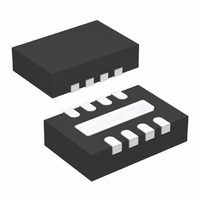
LTC6102HDD#PBF Linear Technology, LTC6102HDD#PBF Datasheet - Page 17

LTC6102HDD#PBF
Manufacturer Part Number
LTC6102HDD#PBF
Description
IC AMP CURRENT SENSE 8-DFN
Manufacturer
Linear Technology
Datasheet
1.LTC6102CDDPBF.pdf
(26 pages)
Specifications of LTC6102HDD#PBF
Amplifier Type
Current Sense
Number Of Circuits
1
Gain Bandwidth Product
200kHz
Current - Input Bias
60pA
Voltage - Input Offset
3µV
Current - Supply
420µA
Current - Output / Channel
1mA
Voltage - Supply, Single/dual (±)
4 V ~ 60 V
Operating Temperature
-40°C ~ 125°C
Mounting Type
Surface Mount
Package / Case
8-DFN
Lead Free Status / RoHS Status
Lead free / RoHS Compliant
Output Type
-
-3db Bandwidth
-
Slew Rate
-
Available stocks
Company
Part Number
Manufacturer
Quantity
Price
APPLICATIONS INFORMATION
Output Filtering
The output voltage, V
makes fi ltering straightforward. Any circuit may be used
which generates the required Z
response. For example, a capacitor in parallel with R
will give a low pass response. This will reduce unwanted
noise from the output, and may also be useful as a charge
reservoir to keep the output steady while driving a switch-
ing circuit such as a mux or ADC. This output capacitor
in parallel with an output resistor will create a pole in the
output response at:
Useful Equations
Input Sense Range
The inputs of the LTC6102 can function from V
Not only does this allow a wide V
the input reference to be separate from the positive supply
(Figure 6). Note that the difference between V
must be no more than the input sense voltage range listed
in the Electrical Characteristics table.
Monitoring Voltages Above V
The LTC6102 may be confi gured to monitor voltages that are
higher than its supply, provided that the negative terminal
of the input voltage is within the input sense range of the
LTC6102. Figure 7 illustrates a circuit in which the LTC6102
has its supply pin tied to the lower potential terminal of the
sense resistor instead of the higher potential terminal. The
Input Voltage: V
Current Gain:
Transconductance:
Transimpedance:
f
Voltage
–
3
dB
=
2
G G ain:
• •
π
R
I
V
S
I
OUT
SENSE
V
OUT
SENSE
E E NSE
1
OUT
I
SENSE
V
OUT
•
V
OUT
C
=
I
SENSE
=I
OUT
OUT
=
, is simply I
R
SENSE
R
SENSE
R
R
=
OUT
+
OUT
IN
IN
R
SENSE
=
and Level Translation
SENSE
R
•
to get the desired fi lter
1 1
R
IN
SENSE
range, it also allows
•
OUT
R
R
OUT
I I N
+
• Z
to (V
BAT
OUT
+
and V
. This
– 2V).
OUT
+
operation of the LTC6102 is such that the –INS and –INF
pins will servo to within a few microvolts of +IN, which is
shorted to V
includes V
across R
causing current V
the supply current of the LTC6102 is also monitored, as
it fl ows through R
Because the voltage across R
the sense range of the LTC6102 in this circuit, V
can be large compared to the allowed sense voltage. This
facilitates the sensing of very large voltages, provided
that R
Figure 6. V
Figure 7. LTC6102 Supply Current Monitored with Load
R
(V
SENSE
IN
+
– 2V) TO V
LOAD
LOAD
V
SENSE
is chosen so that V
V
BAT
BAT
LTC6102-1/LTC6102HV
+
R
, the circuit will operate properly. The voltage
+
SENSE
+
. Since the input sense range of the LTC6102
R
Powered Separately from Load Supply (V
R
+
IN
IN
will be held across R
+IN
+IN
V
V
SENSE
SENSE
–
–
LTC6102
LTC6102
/R
.
+
+
IN
to fl ow to R
SENSE
–
–
SENSE
/R
IN
IN
is not restricted to
V
OUT
–INS
–INF
V
V
OUT
–INS
–INF
V
REG
6102 F06
+
REG
LTC6102
+
does not exceed
by the LTC6102,
OUT
. In this case,
R
R
OUT
OUT
V
0.1μF
0.1 F
V
+
V
OUT
6102 F07
OUT
17
BAT
SENSE
6102fd
)


