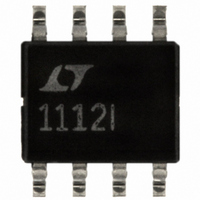
LT1112IS8#PBF Linear Technology, LT1112IS8#PBF Datasheet - Page 6

LT1112IS8#PBF
Manufacturer Part Number
LT1112IS8#PBF
Description
IC OP AMP PREC DUAL LOPWR 8-SOIC
Manufacturer
Linear Technology
Type
General Purpose Amplifierr
Datasheet
1.LT1112CN8PBF.pdf
(16 pages)
Specifications of LT1112IS8#PBF
Amplifier Type
General Purpose
Number Of Circuits
2
Slew Rate
0.3 V/µs
Gain Bandwidth Product
750kHz
Current - Input Bias
100pA
Voltage - Input Offset
25µV
Current - Supply
350µA
Voltage - Supply, Single/dual (±)
2 V ~ 40 V, ±1 V ~ 20 V
Operating Temperature
-40°C ~ 85°C
Mounting Type
Surface Mount
Package / Case
8-SOIC (3.9mm Width)
Rail/rail I/o Type
No
Number Of Elements
2
Unity Gain Bandwidth Product
0.75MHz
Common Mode Rejection Ratio
115dB
Input Offset Voltage
75uV
Input Bias Current
280pA
Single Supply Voltage (typ)
Not RequiredV
Dual Supply Voltage (typ)
±3/±5/±9/±12/±15/±18V
Voltage Gain In Db
133.98dB
Power Supply Rejection Ratio
114dB
Power Supply Requirement
Dual
Shut Down Feature
No
Single Supply Voltage (min)
Not RequiredV
Single Supply Voltage (max)
Not RequiredV
Dual Supply Voltage (min)
±1V
Dual Supply Voltage (max)
±20V
Technology
Bipolar
Operating Temp Range
-40C to 85C
Operating Temperature Classification
Industrial
Mounting
Surface Mount
Pin Count
8
Package Type
SOIC N
Lead Free Status / RoHS Status
Lead free / RoHS Compliant
Output Type
-
Current - Output / Channel
-
-3db Bandwidth
-
Lead Free Status / Rohs Status
Compliant
Available stocks
Company
Part Number
Manufacturer
Quantity
Price
LT1112/LT1114
ELECTRICAL CHARACTERISTICS
Note 5: Offset voltage, supply current and power supply rejection ratio are
measured at the minimum supply voltage.
Note 6: Matching parameters are the difference between amplifiers A and
D and between B and C on the LT1114; between the two amplifiers on the
LT1112.
Note 7: This parameter is the difference between two noninverting input
bias currents.
Note 8: ∆CMRR and ∆PSRR are defined as follows: (1) CMRR and PSRR
are measured in µV/V on the individual amplifiers. (2) The difference is
calculated between the matching sides in µV/V. (3) The result is converted
to dB.
Note 9: This parameter is not 100% tested.
6
TYPICAL PERFOR A CE CHARACTERISTICS
–100
–200
100
200
OFFSET VOLTAGE DRIFT WITH TEMPERATURE (µV/°C)
15
10
20
0
0
5
–0.8
–75
Input Bias and Offset Current,
Noninverting Bias Current Match
vs Temperature
Drift with Temperature
LT1112N8/J8, LT1114J
850 OP AMPS TESTED
100 LT1112J8
165 LT1112N8
80 LT1114J
V
S
–0.6
–50 –25
= ±15V
–0.4
I
B
TEMPERATURE (°C)
(OVERCANCELLED)
–0.2
0
I
B
(UNDERCANCELLED)
25
0
0.2
50
75
0.4
W
LT1112/14 • TPC04
V
LT1112/14 • TPC01
∆I
S
B
= ±15V
100 125
+
0.6
I
OS
U
0.8
–100
–150
150
100
–50
50
15
OFFSET VOLTAGE DRIFT WITH TEMPERATURE (µV/°C)
25
20
10
0
0
5
–15
–1.4
Input Bias Current Over
Common Mode Range
Drift with Temperature
LT1112S8, LT1114N/S
960 OP AMPS TESTED
240 LT1112S8
80 LT1114N
40 LT1114S
V
T
R
S
A
INCM
DEVICE WITH POSITIVE INPUT CURRENT
DEVICE WITH NEGATIVE INPUT CURRENT
= 25°C
COMMON MODE INPUT VOLTAGE (V)
–1.0
= ±15V
–10
= 800GΩ
–0.6
–5
–0.2
Note 10: These parameters are not tested. More than 99% of the op amps
tested during product characterization have passed the maximum limits.
100% passed at 1kHz.
Note 11: The LT1112AC/LT1112C/LT1112S8/LT1112I and LT1114AC/
LT1114C/LT1114S/LT1114I are guaranteed functional over the
temperature range of –40°C to 85°C.
Note 12: The LT1112AC/LT1112C/LT1112S8/LT1114AC/LT1114C/
LT1114S are guaranteed to meet specified performance from 0°C to 70°C
and are designed, characterized and expected to meet specified
performance from –40°C to 85°C, but are not tested or QA sampled at
these temperatures. The LT1112I/LT1114I are guaranteed to meet
specified performance from –40°C to 85°C.
0
V CM
0.2
I
B
5
0.6
–
+
V
LT1112/14 • TPC02
LT1112/14 • TPC05
S
= ±15V
10
1.0
1.4
15
30
20
10
20
10
30
25
15
0
0
5
–300
–80
Distribution of Input Bias Current
(In All Packages Except LT1114S)
Distribution of Offset Voltage at
V
S
V
T
T
A
S
A
–60
= ±1.0V (In All Packages)
= 25°C
= ±15V
= 25°C
–200 –100
–40
INPUT OFFSET VOLTAGE (µV)
INPUT BIAS CURRENT (pA)
–20
0
0
20
100
40
LT1112/14 • TPC06
60
LT1112/14 • TPC03
200
111214fb
80
300
100


