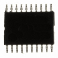
NJM2710V-TE1 NJR, NJM2710V-TE1 Datasheet

NJM2710V-TE1
Specifications of NJM2710V-TE1
NJM2710V-TE1TR
Available stocks
Related parts for NJM2710V-TE1
NJM2710V-TE1 Summary of contents
Page 1
... R = (75dB typ.) DMP20,SSOP20 20 19 Pin Function OUTPUT 2. A -INPUT - +INPUT + OUTPUT -INPUT +INPUT OUTPUT -INPUT 10. C +INPUT PACKAGR OUTLINE NJM2710M NJM2710V 11. D OUTPUT 12. D -INPUT 13. D +INPUT 14. E OUTPUT 15. E -INPUT 16. E +INPUT - 17. V 18. F OUTPUT 19. F -INPUT 20. F +INPUT - 1 - ...
Page 2
ABSOLUTE MAXIMUM RATINGS PARAMETER Supply Voltage Differential Input Voltage Power Dissipation Operating Temperature Range Storage Temperature Range DC CHARACTERISTICS PARAMETER Operating Voltage Range Operating Current Input Offset Voltage Input Bias Current Input Offset Current Open Loop Voltage Gain Input Common ...
Page 3
Note: non-inverting amplifier 1.The closed gain should be 6dB or higher to prevent the oscillation. Unity gain follower application may cause the oscillation. 2.When the closed gain is lower than 20dB, use a compensation capacitor (CF: about 5pF), parallel with ...
Page 4
TYPICAL CHARACTRERISTICS Supply Current vs. Supply Voltage V =No Signal,G =6dB =1kΩ,R =1kΩ,R =2kΩ,Ta=+ 1.0 2.0 3.0 Supply Voltage ±V [V] Input Offset ...
Page 5
TYPICAL CHARACTRERISTICS + V Common Mode Rejection Ratio vs. Ambient Temperature + - V /V =2.5V 120 110 100 -50 - Ambient Temperature [ Maximum Output Voltage vs. Load Resistance + - V ...
Page 6
TYPICAL CHARACTRERISTICS Pulse Responce + - V /V =±2.5V,f=5MHz,V =2VPP,G =6dB =1kΩ,C =5pF,R =1kΩ,R =2kΩ,C =10pF,Ta=+25℃ 1.0 0.0 -1.0 -2.0 -3.0 -4.0 -5.0 0.0 0.0 0.1 0.1 0.1 0.1 Time [10ns/div] Pulse ...
Page 7
TYPICAL CHARACTRERISTICS Voltage Gain vs. Frequency (correlation with RL =±2.5V,V =0.02Vpp,G =40dB =1.98kΩ,R =20Ω,C =5pF Gain Phase -10 -20 -30 RL=1kΩ -40 100k ...
Page 8
MEASUREMENT CIRCUIT - 8 - DUT [CAUTION] The specifications on this databook are only given for information , without any guarantee as regards either mistakes or omissions. The application circuits in this databook are described ...


