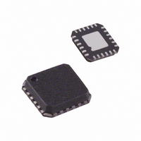
ADA4932-2YCPZ-R2 Analog Devices Inc, ADA4932-2YCPZ-R2 Datasheet - Page 20

ADA4932-2YCPZ-R2
Manufacturer Part Number
ADA4932-2YCPZ-R2
Description
IC AMP DIFF DUAL LP 80MA 24LFCSP
Manufacturer
Analog Devices Inc
Datasheet
1.ADA4932-1YCPZ-R7.pdf
(28 pages)
Specifications of ADA4932-2YCPZ-R2
Amplifier Type
Differential
Number Of Circuits
2
Output Type
Differential
Slew Rate
2800 V/µs
-3db Bandwidth
560MHz
Current - Input Bias
2.5µA
Voltage - Input Offset
500µV
Current - Supply
9.6mA
Current - Output / Channel
80mA
Voltage - Supply, Single/dual (±)
3 V ~ 11 V, ±1.5 V ~ 5.5 V
Operating Temperature
-40°C ~ 105°C
Mounting Type
Surface Mount
Package / Case
24-LFCSP
No. Of Amplifiers
2
Input Offset Voltage
2.2mV
Bandwidth
560MHz
Supply Voltage Range
3V To 11V
Supply Current
9.6mA
Amplifier Case Style
LFCSP
No. Of Pins
16
Rohs Compliant
Yes
Lead Free Status / RoHS Status
Lead free / RoHS Compliant
Gain Bandwidth Product
-
Other names
ADA4932-2YCPZ-R2TR
ADA4932-1/ADA4932-2
APPLICATIONS INFORMATION
ANALYZING AN APPLICATION CIRCUIT
The ADA4932-x uses high open-loop gain and negative feedback
to force its differential and common-mode output voltages in
such a way as to minimize the differential and common-mode
error voltages. The differential error voltage is defined as the
voltage between the differential inputs labeled +IN and −IN
(see Figure 55). For most purposes, this voltage can be assumed
to be zero. Similarly, the difference between the actual output
common-mode voltage and the voltage applied to V
be assumed to be zero. Starting from these principles, any applica-
tion circuit can be analyzed.
SETTING THE CLOSED-LOOP GAIN
Using the approach described in the Analyzing an Application
Circuit section, the differential gain of the circuit in Figure 55
can be determined by
This presumes that the input resistors (R
(R
ESTIMATING THE OUTPUT NOISE VOLTAGE
The differential output noise of the ADA4932-x can be
estimated using the noise model in Figure 56. The input-
referred noise voltage density, v
Table 11. Output Noise Voltage Density Calculations for Matched Feedback Networks
Input Noise Contribution
Differential Input
Inverting Input
Noninverting Input
V
Gain Resistor, R
Gain Resistor, R
Feedback Resistor, R
Feedback Resistor, R
Table 12. Differential Input, DC-Coupled
Nominal Gain (dB)
0
6
10
Table 13. Single-Ended Ground-Referenced Input, DC-Coupled, R
Nominal Gain (dB)
0
6
10
1
R
OCM
G2
F
) on each side are equal.
= R
Input
V
V
G1
OUT
IN
+ (R
,
,
dm
dm
S
||R
T
).
G1
G2
R
R
G
F
F1
F2
R
511
523
806
F
(Ω)
nIN
R
499
249
243
R
499
499
768
, is modeled as a differential
Input Noise Term
v
i
i
v
v
v
v
v
G1
nIN−
nIN+
nIN
nCM
nRG1
nRG2
nRF1
nRF2
F
(Ω)
(Ω)
G
) and feedback resistors
R
53.6
57.6
57.6
T
(Ω) (Std 1%) R
R
499
249
243
G
(Ω)
OCM
can also
Input Noise
Voltage Density
v
i
i
v
(4kTR
(4kTR
(4kTR
(4kTR
R
998
498
486
nIN−
nIN+
nIN
nCM
IN, dm
665
374
392
Rev. A | Page 20 of 28
IN, cm
× (R
× (R
G1
G2
F1
F2
(Ω)
)
)
)
)
1/2
1/2
1/2
1/2
F2
F1
(Ω)
)
)
S
= 50 Ω
Differential Output Noise Density (nV/√Hz)
9.25
12.9
18.2
R
525
276
270
input, and the noise currents, i
each input and ground. The output voltage due to v
by multiplying v
equation that follows). The noise currents are uncorrelated with
the same mean-square value, and each produces an output voltage
that is equal to the noise current multiplied by the associated
feedback resistance. The noise voltage density at the V
v
as is true in most cases, the output noise due to v
mode. Each of the four resistors contributes (4kTR
noise from the feedback resistors appears directly at the output,
and the noise from the gain resistors appears at the output multip-
lied by R
multiplication factors, and the output-referred noise density terms.
nCM
G2
(Ω)
. When the feedback networks have the same feedback factor,
1
Output
Multiplication Factor
G
1
1
0
R
R
1
1
F1
F2
F
N
/R
/R
/R
G
G1
G2
V
V
. Table 11 summarizes the input noise sources, the
Differential Output Noise Density (nV/√Hz)
9.19
12.6
17.7
nRG1
nRG2
nIN
R
R
i
i
by the noise gain, G
G1
G2
nIN+
nIN–
Figure 56. Noise Model
V
nIN
R
R
F1
F2
ADA4932-x
nIN−
+
and i
V
V
V
nRF1
OCM
nRF2
Differential Output Noise
Voltage Density Term
v
v
v
v
v
v
v
v
nO1
nO2
nO3
nO4
nO5
nO6
nO7
nO8
N
nIN+
= G
= (i
= (i
= 0 V
= (R
= (R
= (4kTR
= (4kTR
(defined in the G
, appear between
nIN−
nIN+
N
F1
F2
V
(v
/R
/R
nOD
V
)(R
)(R
nIN
nCM
G1
G2
F1
F2
)
nCM
F2
F1
)
)
)(4kTR
)(4kTR
nIN
1/2
1/2
)
)
xx
)
is obtained
is common
1/2
OCM
. The
G1
G2
)
)
1/2
1/2
pin is
N


