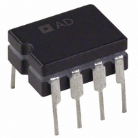
AD708AQ Analog Devices Inc, AD708AQ Datasheet

AD708AQ
Specifications of AD708AQ
Available stocks
Related parts for AD708AQ
AD708AQ Summary of contents
Page 1
FEATURES Very high dc precision 30 μV maximum offset voltage 0.3 μV/°C maximum offset voltage drift 0.35 μV p-p maximum voltage noise (0 Hz) 5 million V/V minimum open-loop gain 130 dB minimum CMRR 120 dB minimum ...
Page 2
AD708 TABLE OF CONTENTS Features .............................................................................................. 1 Pin Configuration............................................................................. 1 General Description ......................................................................... 1 Product Highlights ........................................................................... 1 Revision History ............................................................................... 2 Specifications..................................................................................... 3 Absolute Maximum Ratings............................................................ 5 ESD Caution.................................................................................. 5 Typical Performance Characteristics ............................................. 6 Matching Characteristics............................................................. 9 REVISION ...
Page 3
SPECIFICATIONS @ 25°C and ±15 V dc, unless otherwise noted. Table 1. Parameter Conditions 2 INPUT OFFSET VOLTAGE T MIN Drift Long Term Stability INPUT BIAS CURRENT T MIN Average Drift OFFSET CURRENT V T MIN Average Drift 3 MATCHING ...
Page 4
AD708 Parameter Conditions OUTPUT VOLTAGE MIN OPEN-LOOP OUTPUT RESISTANCE POWER SUPPLY Quiescent Current Power Consumption V V Operating Range 1 All min and max specifications are guaranteed. Specifications in boldface are tested on all production units ...
Page 5
ABSOLUTE MAXIMUM RATINGS Table 2. Parameter Supply Voltage 1 Internal Power Dissipation 2 Input Voltage Output Short-Circuit Duration Differential Input Voltage Storage Temperature Range (Q) Storage Temperature Range (N) Lead Temperature (Soldering 60 sec) 1 Thermal Characteristics 8-lead PDIP: θ ...
Page 6
AD708 TYPICAL PERFORMANCE CHARACTERISTICS V = ±15 V and T = 25°C, unless otherwise noted –0.5 +V –1.0 –1.5 1.5 1.0 –V 0.5 – SUPPLY VOLTAGE (±V) Figure 2. Input Common-Mode ...
Page 7
DIFFERENTIAL VOLTAGE (±V) Figure 8. Input Bias Current vs. Differential Input Voltage 1/F CORNER 20 0.7Hz 0 ...
Page 8
AD708 160 140 120 100 0 100 1k FREQUENCY (Hz) Figure 14. Common-Mode Rejection vs. Frequency 2.8kHz MAX 10k FREQUENCY (Hz) Figure ...
Page 9
MATCHING CHARACTERISTICS 32 25° –50 –40 –30 –20 – OFFSET VOLTAGE MATCH (µV) Figure 19. Typical Distribution of Offset Voltage Match 32 –55°C TO +125° ...
Page 10
AD708 THEORY OF OPERATION CROSSTALK PERFORMANCE The AD708 exhibits very low crosstalk as shown in Figure 25, Figure 26, and Figure 27. Figure 25 shows the offset voltage induced on Side B of the AD708 when Side A output is ...
Page 11
OPERATION WITH A GAIN OF −100 To show the outstanding dc precision of the AD708 in a real application, Table 3 shows an error budget calculation for a gain of −100. This configuration is shown in Figure 28. Table 3. ...
Page 12
AD708 BRIDGE SIGNAL CONDITIONER The AD708 can be used in the circuit shown in Figure 30 to produce an accurate and inexpensive dynamic bridge condi- tioner. The low offset voltage match and low offset voltage drift match of the AD708 ...
Page 13
... Dimensions shown in inches and (millimeters) ORDERING GUIDE Model Temperature Range AD708JN 0°C to +70°C 1 AD708JNZ 0°C to +70°C AD708AQ −40°C to +85°C AD708BQ −40°C to +85°C AD708SQ/883B −55°C to +125° Pb-free part. 0.325 (8.26) 0.310 (7.87) 0.300 (7.62) ...
Page 14
AD708 NOTES Rev Page ...
Page 15
NOTES Rev Page AD708 ...
Page 16
AD708 NOTES ©2006 Analog Devices, Inc. All rights reserved. Trademarks and registered trademarks are the property of their respective owners. C05789-0-1/06(C) Rev Page ...


