OP200EZ Analog Devices Inc, OP200EZ Datasheet
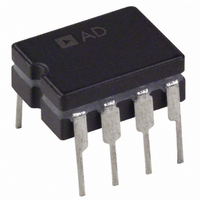
IC OPAMP GP 500KHZ DUAL LP 8CDIP

OP200EZ

Manufacturer Part Number
OP200EZ
Description
IC OPAMP GP 500KHZ DUAL LP 8CDIP
Manufacturer
Analog Devices Inc
Datasheets

Specifications of OP200EZ

Slew Rate
0.15 V/µs
Rohs Status
RoHS non-compliant
Amplifier Type
General Purpose
Number Of Circuits
2
Gain Bandwidth Product
500kHz
Current - Input Bias
100pA
Voltage - Input Offset
25µV
Current - Supply
570µA
Voltage - Supply, Single/dual (±)
±3 V ~ 18 V
Operating Temperature
-40°C ~ 85°C
Mounting Type
Through Hole
Package / Case
8-CDIP (0.300", 7.62mm)
Op Amp Type
Low Offset Voltage
No. Of Amplifiers
2
Bandwidth
500kHz
Supply Voltage Range
± 3V To ± 18V
Amplifier Case Style
DIP
No. Of Pins
8
Rail/rail I/o Type
No
Number Of Elements
2
Unity Gain Bandwidth Product
0.5MHz
Common Mode Rejection Ratio
120dB
Input Offset Voltage
0.075@±15VmV
Input Bias Current
2nA
Single Supply Voltage (typ)
Not RequiredV
Dual Supply Voltage (typ)
±5/±9/±12/±15V
Voltage Gain In Db
140dB
Power Supply Requirement
Dual
Shut Down Feature
No
Single Supply Voltage (min)
Not RequiredV
Single Supply Voltage (max)
Not RequiredV
Dual Supply Voltage (min)
±3V
Dual Supply Voltage (max)
±20V
Technology
Bipolar
Operating Temp Range
-40C to 85C
Operating Temperature Classification
Industrial
Mounting
Through Hole
Pin Count
8
Package Type
CDIP
Channel Separation
145
Current, Input Bias
0.1 nA
Current, Input Offset
0.05 nA
Current, Supply
570 μA
Impedance, Thermal
16 °C/W
Number Of Amplifiers
Dual
Resistance, Input
10 Megohms (Differential), 125 Gigaohms (Common-Mode)
Temperature, Operating, Range
-40 to +85 °C
Voltage, Gain
12000 V/mV
Voltage, Input
±13 V
Voltage, Noise
22 nV/sqrt Hz
Voltage, Offset
25 μV
Voltage, Output, High
+12.2 V
Voltage, Output, Low
-12.2 V
Voltage, Supply
±15 V
Output Type
-
Current - Output / Channel
-
-3db Bandwidth
-
Lead Free Status / Rohs Status
Not Compliant

Available stocks

Company
Part Number
Manufacturer
Quantity
Price
Part Number:
OP200EZ
Manufacturer:
PMI
Quantity:
5 510
Part Number:
OP200EZ
Manufacturer:
ADI/亚德诺
Quantity:
20 000
Part Number:
OP200EZ/FZ
Manufacturer:
PMI
Quantity:
5 510
Part Number:
OP200EZ/FZ
Manufacturer:
OMRON
Quantity:
5 510
a
Information furnished by Analog Devices is believed to be accurate and
reliable. However, no responsibility is assumed by Analog Devices for its
use, nor for any infringements of patents or other rights of third parties that
may result from its use. No license is granted by implication or otherwise
under any patent or patent rights of Analog Devices. Trademarks and
registered trademarks are the property of their respective owners.
GENERAL DESCRIPTION
The OP200 is the first monolithic dual operational amplifier to
offer OP77 type precision performance. Available in the industry-
standard 8-lead pinout, the OP200 combines precision performance
with the space and cost savings offered by a dual amplifier.
The OP200 features an extremely low input offset voltage of less
than 75 µV with a drift below 0.5 µV/°C, guaranteed over the full
military temperature range. Open-loop gain of the OP200 exceeds
5,000,000 into a 10 kΩ load; input bias current is under 2 nA;
CMR is over 120 dB and PSRR below 1.8 µV/V. On-chip
Zener zap trimming is used to achieve the extremely low input
offset voltage of the OP200 and eliminates the need for offset
pulling.
Power consumption of the OP200 is very low, with each amplifier
drawing less than 725 µA of supply current. The total current
drawn by the dual OP200 is less than one-half that of a single
OP07, yet the OP200 offers significant improvements over this
industry-standard op amp. The voltage noise density of the OP200,
11 nV/√Hz at 1 kHz, is half that of most competitive devices.
REV. B
FEATURES
Low Input Offset Voltage: 75 V Max
Low Offset Voltage Drift, Over –55 C < T
Low Supply Current (Per Amplifier): 725 A Max
High Open-Loop Gain: 5000 V/mV Min
Low Input Bias Current: 2 nA Max
Low Noise Voltage Density: 11 nV/√Hz at 1 kHz
Stable with Large Capacitive Loads: 10 nF Typ
Pin Compatible to OP221, MC1458, and LT1013 with
Available in Die Form
0.5 V/ C Max
Improved Performance
+IN
Figure 1. Simplified Schematic (One of two amplifiers is shown.)
NETWORK
VOLTAGE
LIMITING
–IN
A
< +125 C:
The OP200 is pin compatible with the OP221, LM158,
MC1458/1558, and LT1013.
The OP200 is an ideal choice for applications requiring multiple
precision op amps and where low power consumption is critical.
For a quad precision op amp, see the OP400.
One Technology Way, P.O. Box 9106, Norwood, MA 02062-9106, U.S.A.
Tel: 781/329-4700
Fax: 781/326-8703
Dual Low Offset, Low Power
OUT A
BIAS
8-Lead CERDIP (Z-Suffix)
–IN A
+IN A
16-Lead SOIC (S - Suffix)
8-Lead PDIP (P-Suffix)
–IN A
+IN A
+IN B
–IN B
PIN CONNECTIONS
V–
NC
NC
NC
V–
© 2004 Analog Devices, Inc. All rights reserved.
Operational Amplifier
1
2
3
4
NC = NO CONNECT
1
2
3
4
5
6
7
8
A
+
+ –
B
16
15
14
13
12
11
10
9
8
7
6
5
OUT A
NC
NC
V+
NC
NC
OUT B
NC
V+
OUT B
–IN B
+IN B
OUT
V+
V–
OP200
www.analog.com

Related parts for OP200EZ

OP200EZ Summary of contents

Page 1

FEATURES Low Input Offset Voltage Max Low Offset Voltage Drift, Over –55 C < Max Low Supply Current (Per Amplifier): 725 A Max High Open-Loop Gain: 5000 V/mV Min Low Input Bias Current: ...

Page 2

OP200–SPECIFICATIONS ELECTRICAL CHARACTERISTICS Parameter Symbol Conditions Input Offset Voltage V OS Long-Term Input Voltage Stability Input Offset Current Input Bias Current Input Noise Voltage e 0 p-p Input Noise ...

Page 3

ELECTRICAL CHARACTERISTICS Parameter Input Offset Voltage Average Input Offset Voltage Drift Input Offset Current Input Bias Current Large Signal Voltage Gain Input Voltage Range* Common-Mode Rejection Power Supply Rejection Ratio Output Voltage Swing Supply Current Per Amplifier Capacitive Load Stability ...

Page 4

OP200–SPECIFICATIONS ELECTRICAL CHARACTERISTICS Parameter Symbol Conditions Input Offset Voltage V OS Average Input Offset Voltage Drift TCV OS Input Offset Current Input Bias Current Large-Signal V Voltage Gain Input Voltage ...

Page 5

... OP200 100 10k 1/2 TO SPECTRUM e OUT OP200 ANALYZER (nV/ Hz (nV/ Hz 101 OUT OUT Figure 3. Noise Test Schematic ORDERING GUIDE Package Operating CERDIP Temperature 8-Lead Plastic Range OP200AZ MIL OP200EZ XIND OP200GP XIND OP200GS XIND OP200GS-REEL XIND ADI Equivalent OP200ARCMDA OP200AZMDA ...

Page 6

Performance Characteristics OP200 15V TIME – Minutes TPC 1. Warm-Up Drift 300 V = 15V S 250 200 150 100 50 0 ...

Page 7

TWO AMPLIFIERS 1.16 1.14 1.12 1.10 1.08 1. SUPPLY VOLTAGE – V TPC 10. Total Supply Current vs. Supply Voltage 0.7 0.6 0.5 0.4 0.3 0.2 0.1 –75 –50 ...

Page 8

OP200 15V S 40 FALLING RISING 0.5 1.0 1.5 1.0 1.5 3.0 CAPACITIVE LOAD – nF TPC 19. Overshoot vs. Capacitive Load ...

Page 9

... DAC8212AV AGND DAC A/DAC DGND 5 Figure 7. Dual 12-Bit Voltage Output DAC –9– OP200 R3 R1 10k 10k 2 R5 100 1 OP200EZ IN 10k 3 + 1/2 1k OP200EZ 10mA/V OUT 100 RS –15 Figure 6. Precision Current Pump 8 – 1/2 1 OUTA OP200AZ 4 –15V – 1/2 7 OUTB OP200AZ I OUT ...

Page 10

OP200 Dual Precision Voltage Reference A dual OP200 and a REF43, a 2.5 V reference, can be used to build a ± 2.5 V precision voltage reference. Maximum output current from each reference is ± with load regulation ...

Page 11

Ceramic Dual In-Line Package [CERDIP] (Q-8) Z-Suffix Dimensions shown in inches and (millimeters) 0.005 (0.13) 0.055 (1.40) MIN MAX 8 5 0.310 (7.87) 0.220 (5.59) PIN 0.100 (2.54) BSC 0.405 (10.29) MAX 0.060 (1.52) 0.015 (0.38) ...

Page 12

OP200 Revision History Location 2/04—Data Sheet changed from REV REV. B. OP200F deleted . . . . . . . . . . . . . . . . . . . . . . . . . ...

Related keywords