OP27AZ Analog Devices Inc, OP27AZ Datasheet - Page 4
OP27AZ
Manufacturer Part Number
OP27AZ
Description
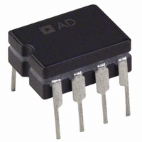
IC OPAMP GP 8MHZ LN PREC 8CDIP
Manufacturer
Analog Devices Inc
Datasheet
1.OP27GSZ.pdf
(20 pages)
Specifications of OP27AZ
Slew Rate
2.8 V/µs
Rohs Status
RoHS non-compliant
Amplifier Type
General Purpose
Number Of Circuits
1
Gain Bandwidth Product
8MHz
Current - Input Bias
10nA
Voltage - Input Offset
10µV
Voltage - Supply, Single/dual (±)
±4 V ~ 18 V
Operating Temperature
-55°C ~ 125°C
Mounting Type
Through Hole
Package / Case
8-CDIP (0.300", 7.62mm)
Op Amp Type
Precision
No. Of Amplifiers
1
Bandwidth
8MHz
Supply Voltage Range
± 4V To ± 18V
Amplifier Case Style
DIP
No. Of Pins
8
Operating Temperature Range
-55°C To +125°C
Current - Supply
-
Output Type
-
Current - Output / Channel
-
-3db Bandwidth
-
Lead Free Status / RoHS Status
Contains lead / RoHS non-compliant
Available stocks
Company
Part Number
Manufacturer
Quantity
Price

Part Number:
OP27AZ/883
Manufacturer:
ADI/亚德诺
Quantity:
20 000
Part Number:
OP27AZ/883C
Manufacturer:
ADI/亚德诺
Quantity:
20 000
Company:
Part Number:
OP27AZ/883C/Q
Manufacturer:
a
Quantity:
19
Part Number:
OP27AZ/883Q
Manufacturer:
ADI/亚德诺
Quantity:
20 000
Part Number:
OP27AZ7
Manufacturer:
ADI/亚德诺
Quantity:
20 000


OP27
SPECIFICATIONS
ELECTRICAL CHARACTERISTICS
V
Table 1.
Parameter
INPUT OFFSET VOLTAGE
LONG-TERM V
INPUT OFFSET CURRENT
INPUT BIAS CURRENT
INPUT NOISE VOLTAGE
INPUT NOISE
INPUT NOISE
INPUT RESISTANCE
INPUT VOLTAGE RANGE
COMMON-MODE REJECTION RATIO
POWER SUPPLY REJECTION RATIO
LARGE SIGNAL VOLTAGE GAIN
OUTPUT VOLTAGE SWING
SLEW RATE
GAIN BANDWIDTH PRODUCT
OPEN-LOOP OUTPUT RESISTANCE
POWER CONSUMPTION
OFFSET ADJUSTMENT RANGE
1
2
3
4
5
6
Input offset voltage measurements are performed approximately 0.5 seconds after application of power. A/E grades guaranteed fully warmed up.
Long-term input offset voltage stability refers to the average trend line of V
hour of operation, changes in V
Sample tested.
See voltage noise test circuit (Figure 31).
Guaranteed by input bias current.
Guaranteed by design.
S
Voltage Density
Current Density
Differential Mode
Common Mode
= ±15 V, T
6
A
OS
= 25°C, unless otherwise noted.
STABILITY
3
3
5
3, 4
1
2, 3
OS
during the first 30 days are typically 2.5 μV. Refer to the Typical Performance Characteristics section.
6
Symbol
V
V
e
e
i
R
R
IVR
PSRR
A
V
SR
GBW
R
P
I
I
CMRR
OS
B
n
n p-p
n
OS
OS
IN
INCM
O
O
d
VO
/Time
Conditions
0.1 Hz to 10 Hz
f
f
f
f
f
f
V
V
R
R
R
R
R
V
V
R
O
O
O
O
O
O
L
L
L
L
L
P
CM
S
O
O
= 10 Hz
= 30 Hz
= 1000 Hz
= 10 Hz
= 30 Hz
= 1000 Hz
= ±4 V to ±18 V
≥ 2 k Ω, V
≥ 600 Ω, V
≥ 2 k Ω
≥ 600 Ω
≥ 2 kΩ
= 10 kΩ
= 0, I
= ±11 V
O
Rev. F | Page 4 of 20
= 0
OS
O
vs. time over extended periods after the first 30 days of operation. Excluding the initial
O
= ±10 V
= ±10 V
Min
1.3
±11.0
114
1000
800
±12.0
±10.0
1.7
5.0
OP27A/E
Typ
10
0.2
7
±10
0.08
3.5
3.1
3.0
1.7
1.0
0.4
6
3
±12.3
126
1
1800
1500
±13.8
±11.5
2.8
8.0
70
90
±4.0
Max
25
1.0
35
±40
0.18
5.5
4.5
3.8
4.0
2.3
0.6
10
140
Min
0.7
±11.0
100
700
600
±11.5
±10.0
1.7
5.0
OP27/G
Typ
30
0.4
12
±15
0.09
3.8
3.3
3.2
1.7
1.0
0.4
4
2
±12.3
120
2
1500
1500
±13.5
±11.5
2.8
8.0
70
100
±4.0
Max
100
2.0
75
±80
0.25
8.0
5.6
4.5
0.6
20
170
Unit
μV
μV/M
nA
nA
μV p-p
nV/√Hz
nV/√Hz
nV/√Hz
pA/√Hz
pA/√Hz
pA/√Hz
MΩ
GΩ
V
dB
μV/V
V/mV
V/mV
V
V
V/μs
MHz
Ω
mW
mV
O
Related parts for OP27AZ
Image
Part Number
Description
Manufacturer
Datasheet
Request
R

Part Number:
Description:
IC OPAMP INSTR PREC SGL 8SOIC
Manufacturer:
Linear Technology
Datasheet:

Part Number:
Description:
Op Amps Low-noise op amp Noise Wide-Band Ampl
Manufacturer:
Maxim Integrated Products
Datasheet:

Part Number:
Description:
Op Amps LW-POW SNGL/DUAL R-R I/O OP AMPS
Manufacturer:
Maxim Integrated Products
Datasheet:
Part Number:
Description:
Op Amps LW-POW SNGL/DUAL R-R I/O OP AMPS
Manufacturer:
Maxim Integrated Products
Datasheet:

Part Number:
Description:
Op Amps Dual Op amp JFET
Manufacturer:
Fairchild Semiconductor
Datasheet:

Part Number:
Description:
Op Amps 1.8V 15MHz Low-Offse set Op Amp with RRIO
Manufacturer:
Maxim Integrated Products
Datasheet:

Part Number:
Description:
Op Amps Ultra low-power op a mp in 6-bump WLP pac
Manufacturer:
Maxim Integrated Products
Datasheet:
Part Number:
Description:
Op Amps 1.8V 15MHz Low-Offse set Op Amp with RRIO
Manufacturer:
Maxim Integrated Products
Datasheet:

Part Number:
Description:
Op Amps Dual High-Voltage Op Amp
Manufacturer:
Maxim Integrated Products
Datasheet:


