AD624BDZ Analog Devices Inc, AD624BDZ Datasheet - Page 11
AD624BDZ
Manufacturer Part Number
AD624BDZ
Description
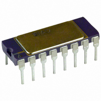
IC AMP INST 25MHZ PREC LN 16CDIP
Manufacturer
Analog Devices Inc
Datasheet
1.AD624ADZ.pdf
(16 pages)
Specifications of AD624BDZ
Amplifier Type
Instrumentation
Number Of Circuits
1
Slew Rate
5 V/µs
Gain Bandwidth Product
25MHz
-3db Bandwidth
1MHz
Current - Input Bias
25nA
Voltage - Input Offset
75µV
Current - Supply
3.5mA
Voltage - Supply, Single/dual (±)
±6 V ~ 18 V
Operating Temperature
-25°C ~ 85°C
Mounting Type
Through Hole
Package / Case
16-CDIP (0.300", 7.62mm)
No. Of Amplifiers
1
Input Offset Voltage
75µV
Gain Db Min
1dB
Bandwidth
25MHz
Amplifier Output
Single Ended
Cmrr
120dB
Supply Voltage Range
± 6V To ± 18V
Rohs Compliant
Yes
Lead Free Status / RoHS Status
Lead free / RoHS Compliant
Output Type
-
Current - Output / Channel
-
Available stocks
Company
Part Number
Manufacturer
Quantity
Price

Part Number:
AD624BDZ
Manufacturer:
ADI/亚德诺
Quantity:
20 000


By establishing a reference at the “low” side of a current setting
resistor, an output current may be defined as a function of input
voltage, gain and the value of that resistor. Since only a small
current is demanded at the input of the buffer amplifier A2, the
forced current I
drift specifications of A2 must be added to the output offset and
drift specifications of the IA.
PROGRAMMABLE GAIN
Figure 38 shows the AD624 being used as a software program-
mable gain amplifier. Gain switching can be accomplished with
mechanical switches such as DIP switches or reed relays. It
should be noted that the “on” resistance of the switch in series
with the internal gain resistor becomes part of the gain equation
and will have an effect on gain accuracy.
A significant advantage in using the internal gain resistors in a
programmable gain configuration is the minimization of thermo-
couple signals which are often present in multiplexed data
acquisition systems.
If the full performance of the AD624 is to be achieved, the user
must be extremely careful in designing and laying out his circuit
to minimize the remaining thermocouple signals.
The AD624 can also be connected for gain in the output stage.
Figure 39 shows an AD547 used as an active attenuator in the
output amplifier’s feedback loop. The active attenuation pre-
sents a very low impedance to the feedback resistors therefore
minimizing the common-mode rejection ratio degradation.
Another method for developing the switching scheme is to use a
DAC. The AD7528 dual DAC which acts essentially as a pair of
switched resistive attenuators having high analog linearity and
COMMON
ANALOG
+V
–V
+IN
–IN
S
S
L
1 F
will largely flow through the load. Offset and
35V
A B
0
0
1
1
GAIN TABLE
C1
0
1
0
1
OFFSET
INPUT
GAIN
TRIM
10k
C2
100
500
200
1
R1
K1 – K3 =
THERMOSEN DM2C
4.5V COIL
D1 – D3 = IN4148
1
2
3
4
5
6
7
8
10k
AD624
20k
50
50
10k
V
B
INPUTS
RANGE
GAIN
10k
20k
+5V
10k
A
B
225.3
80.2
4445.7
124
DECODER
symmetrical bipolar transmission is ideal in this application. The
multiplying DAC’s advantage is that it can handle inputs of
either polarity or zero without affecting the programmed gain.
The circuit shown uses an AD7528 to set the gain (DAC A) and
to perform a fine adjustment (DAC B).
74LS138
–IN
+IN
16
15
14
13
12
11
10
9
–V
+V
1 F
S
S
35V
(+INPUT)
(–INPUT)
OFFSET
OUTPUT
OFFSET
TRIM
R2
10k
INPUT
OUT
NULL
10k
AD711
SHIELDS
1
2
3
4
5
6
7
8
RELAY
+V
–V
10pF
Y0
Y1
Y2
S
S
AD624
20k
10k
NC
50
G = 100
K1
50
K1
10k
D1
V
G = 200
B
K2
V
A1
K2
SS
BUFFER
DRIVER
A2
7407N
AD7590
10k
D2
G = 500
20k
A3
V
K3
DD
K3
A4
10k
GND
WR
D3
80.2
225.3
4445.7
124
39.2k
10 F
28.7k
316k
+5V
LOGIC
COMMON
AD624
16
15
14
13
12
11
10
9
10k
OUTPUT
OFFSET
NULL
1k
1k
1k
TO –V
V
OUT
Related parts for AD624BDZ
Image
Part Number
Description
Manufacturer
Datasheet
Request
R

Part Number:
Description:
±1.7g Dual-Axis IMEMS Accelerometer Evaluation Board
Manufacturer:
Analog Devices Inc
Datasheet:

Part Number:
Description:
Inertial Sensor Evaluation System
Manufacturer:
Analog Devices Inc
Datasheet:
Part Number:
Description:
Manufacturer:
Analog Devices Inc
Datasheet:
Part Number:
Description:
Manufacturer:
Analog Devices Inc
Datasheet:
Part Number:
Description:
Manufacturer:
Analog Devices Inc
Datasheet:
Part Number:
Description:
Manufacturer:
Analog Devices Inc
Datasheet:
Part Number:
Description:
Manufacturer:
Analog Devices Inc
Datasheet:
Part Number:
Description:
Manufacturer:
Analog Devices Inc
Datasheet:
Part Number:
Description:
Manufacturer:
Analog Devices Inc
Datasheet:
Part Number:
Description:
Manufacturer:
Analog Devices Inc
Datasheet:
Part Number:
Description:
Manufacturer:
Analog Devices Inc
Datasheet:
Part Number:
Description:
Manufacturer:
Analog Devices Inc
Datasheet:
Part Number:
Description:
Manufacturer:
Analog Devices Inc
Datasheet: