PA88 Cirrus Logic Inc, PA88 Datasheet - Page 4
PA88
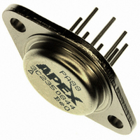
Manufacturer Part Number
PA88
Description
IC PWR AMP 450V 100MA 8PIN TO3
Manufacturer
Cirrus Logic Inc
Series
Apex Precision Power™r
Specifications of PA88
Amplifier Type
Power
Number Of Circuits
1
Slew Rate
30 V/µs
Gain Bandwidth Product
2.1MHz
Current - Input Bias
5pA
Voltage - Input Offset
500µV
Current - Supply
1.7mA
Current - Output / Channel
100mA
Voltage - Supply, Single/dual (±)
30 V ~ 450 V, ±15 V ~ 225 V
Operating Temperature
-25°C ~ 85°C
Mounting Type
Through Hole
Package / Case
TO-3-8
Number Of Channels
1
Voltage Gain Db
111 dB
Common Mode Rejection Ratio (min)
90 dB
Input Offset Voltage
2 mV
Maximum Operating Temperature
+ 85 C
Mounting Style
Through Hole
Maximum Dual Supply Voltage
+/- 225 V
Minimum Operating Temperature
- 25 C
Lead Free Status / RoHS Status
Lead free by exemption / RoHS compliant by exemption
Output Type
-
-3db Bandwidth
-
Lead Free Status / Rohs Status
Details
Other names
598-1328
Available stocks
Company
Part Number
Manufacturer
Quantity
Price

Company:
Part Number:
PA88H
Manufacturer:
LITEON
Quantity:
12 000


PA88 • PA88A
GENERAL
siderations" which covers stability, supplies, heat sinking,
mounting, current limit, SOA interpretation, and specification
interpretation. Visit www.Cirrus.com for design tools that help
automate tasks such as calculations for stability, internal power
dissipation, current limit; heat sink selection; Apex Precision
Power’s complete Application Notes library; Technical Seminar
Workbook; and Evaluation Kits.
CURRENT LIMIT
connected as shown in the external connection diagram. The
minimum value is 3.5 ohm, however for optimum reliability the
resistor value should be set as high as possible. The value
is calculated as follows; with the maximum practical value of
150 ohms.
SAFE OPERATING AREA (SOA)
fier has two distinct limitations:
1. The current handling capability of the MOSFET geometry
2. The junction temperature of the output MOSFETs.
NOTE: The output stage is protected against transient flyback.
However, for protection against sustained, high energy flyback,
external fast-recovery diodes should be used.
4
Please read Application Note 1 "General Operating Con-
For proper operation, the current limit resistor (R
The MOSFET output stage of this power operational ampli-
250
150
100
and the wire bonds.
50
25
15
10
5
25
PULSE CURVES @ 10% DUTY CYCLE MAX
SUPPLY TO OUTPUT DIFFERENTIAL, V
50
R
75
CL
=
100
SOA
I
.7
LIM
125
250
S
–V
CL
O
) must be
(V)
500
P r o d u c t I n n o v a t i o n F r o m
INPUT PROTECTION
up to ±25V, additional external protection is recommended,
and required at total supply voltages above 300 volts. In most
applications 1N4148 or 1N914 signal diodes are sufficient (D1,
D2 in Figure 2a). In more demanding applications where low
leakage or low capacitance are of concern 2N4416 or 2N5457-
2N5459 JFETs connected as diodes will be required (Q1, Q2
in Figure 2b). In either case the input differential voltage will
be clamped to ±.7V. This is sufficient overdrive to produce
maximum power bandwidth.
POWER SUPPLY PROTECTION
mended as protection on the supply pins. The zeners clamp
transients to voltages within the power supply rating and also
clamp power supply reversals to ground. Whether the zeners
are used or not, the system power supply should be evaluated
for transient performance including power-on overshoot and
power-off polarity reversal as well as line regulation.
on either power supply rail should be avoided or protected
against. Reversals or opens on the negative supply rail is
known to induce input stage failure. Unidirectional transzorbs
prevent this, and it is desirable that they be both electrically
and physically as close to the amplifier as possible.
STABILITY
most capacitive loads at a gain of 4 or more, using the rec-
ommended phase
compensation.
nally compensated
and performance can
be tailored to the
application. Use the
graphs of small signal
response and power
response as a guide.
The compensation
capacitor C
be rated at 500V
working voltage. An
NPO capacitor is
recommended. The
compensation net-
work C
mounted closely to
the amplifier pins 7
and 8 to avoid spuri-
ous oscillation.
FIGURE 2. OVERVOLTAGE PROTECTION
Although the PA88 can withstand differential input voltages
Unidirectional zener diode transient suppressors are recom-
Conditions which can cause open circuits or polarity reversals
The PA88 has sufficient phase margin to be stable with
The PA88 is exter-
C
R
C
must be
C
must
–IN
+IN
–IN
+IN
a.
b.
Q1
D1
D2
Q2
5
4
5
4
PA88
PA88
+V
–V
+V
–V
S
S
S
S
3
6
3
6
Z1
Z2
Z1
Z2
PA88U
Related parts for PA88
Image
Part Number
Description
Manufacturer
Datasheet
Request
R

Part Number:
Description:
Development Kit
Manufacturer:
Cirrus Logic Inc
Datasheet:
Part Number:
Description:
Development Kit
Manufacturer:
Cirrus Logic Inc
Datasheet:


Part Number:
Description:
High-efficiency PFC + Fluorescent Lamp Driver Reference Design
Manufacturer:
Cirrus Logic Inc
Datasheet:
Part Number:
Description:
Development Kit
Manufacturer:
Cirrus Logic Inc
Datasheet:
Part Number:
Description:
Development Kit
Manufacturer:
Cirrus Logic Inc
Datasheet:

Part Number:
Description:
Development Kit
Manufacturer:
Cirrus Logic Inc
Datasheet:
Part Number:
Description:
Development Kit
Manufacturer:
Cirrus Logic Inc
Datasheet:
Part Number:
Description:
Development Kit
Manufacturer:
Cirrus Logic Inc
Datasheet:
Part Number:
Description:
Development Kit
Manufacturer:
Cirrus Logic Inc
Datasheet:

Part Number:
Description:
EVALUATION BOARD FOR CS8427
Manufacturer:
Cirrus Logic Inc
Datasheet:

Part Number:
Description:
BOARD EVAL FOR CS8416 RCVR
Manufacturer:
Cirrus Logic Inc
Datasheet:

Part Number:
Description:
EVALUATION BOARD FOR CS8420
Manufacturer:
Cirrus Logic Inc
Datasheet:

Part Number:
Description:
KIT DEVELOPMENT EP9315 ARM9
Manufacturer:
Cirrus Logic Inc
Datasheet:

Part Number:
Description:
KIT DEVELOPMENT EP9302 ARM9
Manufacturer:
Cirrus Logic Inc
Datasheet: