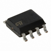
LF351DT STMicroelectronics, LF351DT Datasheet - Page 3

LF351DT
Manufacturer Part Number
LF351DT
Description
IC OPAMP JFET SGL HI SPEED 8SOIC
Manufacturer
STMicroelectronics
Datasheet
1.LF351DT.pdf
(14 pages)
Specifications of LF351DT
Amplifier Type
J-FET
Number Of Circuits
1
Slew Rate
16 V/µs
Gain Bandwidth Product
4MHz
Current - Input Bias
20pA
Voltage - Input Offset
3000µV
Current - Supply
1.4mA
Current - Output / Channel
40mA
Voltage - Supply, Single/dual (±)
6 V ~ 32 V, ±3 V ~ 16 V
Operating Temperature
0°C ~ 70°C
Mounting Type
Surface Mount
Package / Case
8-SOIC (3.9mm Width)
Number Of Channels
1
Common Mode Rejection Ratio (min)
70 dB
Input Offset Voltage
10 mV
Input Bias Current (max)
200 pA
Operating Supply Voltage
5 V, 9 V, 12 V
Supply Current
3.4 mA
Maximum Operating Temperature
+ 70 C
Minimum Operating Temperature
0 C
Dual Supply Voltage
+/- 5 V, +/- 9 V, +/- 12 V, +/- 15 V
Maximum Dual Supply Voltage
+/- 16 V
Minimum Dual Supply Voltage
+/- 3 V
Mounting Style
SMD/SMT
Shutdown
No
Supply Voltage (max)
32 V
Supply Voltage (min)
6 V
Technology
BiFET
Voltage Gain Db
106.02 dB
Lead Free Status / RoHS Status
Lead free / RoHS Compliant
Output Type
-
-3db Bandwidth
-
Lead Free Status / Rohs Status
Lead free / RoHS Compliant
Other names
497-4041-2
Available stocks
Company
Part Number
Manufacturer
Quantity
Price
Company:
Part Number:
LF351DT
Manufacturer:
SIEMENS
Quantity:
6 217
Part Number:
LF351DT
Manufacturer:
ST
Quantity:
20 000
LF351
2
Table 1.
1. All voltage values, except differential voltage, are with respect to the zero reference level (ground) of the supply voltages
2. The magnitude of the input voltage must never exceed the magnitude of the supply voltage or 15 volts, whichever is less.
3. Differential voltages are the non-inverting input terminal with respect to the inverting input terminal.
4. Short-circuits can cause excessive heating and destructive dissipation. Values are typical.
5. The output may be shorted to ground or to either supply. Temperature and/or supply voltages must be limited to ensure
6. Human body model: A 100 pF capacitor is charged to the specified voltage, then discharged through a 1.5 kΩ resistor
7. Machine model: A 200 pF capacitor is charged to the specified voltage, then discharged directly between two pins of the
8. Charged device model: all pins and the package are charged together to the specified voltage and then discharged directly
Table 2.
Symbol
where the zero reference level is the midpoint between V
that the dissipation rating is not exceeded
between two pins of the device. This is done for all couples of connected pin combinations while the other pins are floating.
device with no external series resistor (internal resistor < 5 Ω). This is done for all couples of connected pin combinations
while the other pins are floating.
to the ground through only one pin. This is done for all pins.
Symbol
T
V
oper
R
R
ESD
CC
V
T
V
V
thja
CC
thjc
stg
id
i
Supply voltage
Operating free-air temperature range
Absolute maximum ratings and operating conditions
Absolute maximum ratings
Operating conditions
Supply voltage
Input voltage
Differential input voltage
Thermal resistance junction to ambient
Thermal resistance junction to case
Output short-circuit duration
Storage temperature range
HBM: human body model
MM: machine model
CDM: charged device model
SO-8
DIP8
SO-8
DIP8
(2)
Parameter
(1)
(7)
(3)
(6)
(5)
(8)
Parameter
(4)
Absolute maximum ratings and operating conditions
CC
(4)
+
and V
-55 to +125
LF151
CC
-
.
-40 to +105
6 to 32
LF251
-65 to +150
Infinite
Value
0 to +70
±18
±15
±30
125
500
200
1.5
LF351
85
40
41
°C/W
°C/W
Unit
°C
kV
Unit
V
V
V
V
V
°C
V
3/14


