TS27L4IDT STMicroelectronics, TS27L4IDT Datasheet - Page 4
TS27L4IDT
Manufacturer Part Number
TS27L4IDT
Description
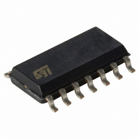
IC AMP PREC LP QUAD OP 14 SOIC
Manufacturer
STMicroelectronics
Specifications of TS27L4IDT
Amplifier Type
General Purpose
Number Of Circuits
4
Slew Rate
0.04 V/µs
Gain Bandwidth Product
100kHz
Current - Input Bias
1pA
Voltage - Input Offset
1100µV
Current - Supply
10µA
Current - Output / Channel
45mA
Voltage - Supply, Single/dual (±)
3 V ~ 16 V, ±1.5 V ~ 8 V
Operating Temperature
-40°C ~ 125°C
Mounting Type
Surface Mount
Package / Case
14-SOIC (3.9mm Width), 14-SOL
Number Of Channels
4
Common Mode Rejection Ratio (min)
65 dB
Input Offset Voltage
10 mV
Input Bias Current (max)
300 pA
Operating Supply Voltage
5 V, 9 V, 12 V, 15 V
Supply Current
0.06 mA
Maximum Operating Temperature
+ 125 C
Minimum Operating Temperature
- 40 C
Mounting Style
SMD/SMT
Shutdown
No
Supply Voltage (max)
16 V
Supply Voltage (min)
3 V
Technology
CMOS
Voltage Gain Db
100 dB
Lead Free Status / RoHS Status
Lead free / RoHS Compliant
Output Type
-
-3db Bandwidth
-
Lead Free Status / Rohs Status
Lead free / RoHS Compliant
Other names
497-2255-2
Available stocks
Company
Part Number
Manufacturer
Quantity
Price
Company:

Part Number:
TS27L4IDT
Manufacturer:
VISHAY
Quantity:
33 000


Absolute maximum ratings and operating conditions
2
4/15
Absolute maximum ratings and operating conditions
Table 1.
1. All values, except differential voltage are with respect to network ground terminal.
2. Differential voltages are the non-inverting input terminal with respect to the inverting input terminal.
3. The magnitude of the input and the output voltages must never exceed the magnitude of the positive
4. Short-circuits can cause excessive heating and destructive dissipation. Values are typical.
5. Human body model: a 100 pF capacitor is charged to the specified voltage, then discharged through a
6. Machine model: a 200 pF capacitor is charged to the specified voltage, then discharged directly between
7. Charged device model: all pins and the package are charged together to the specified voltage and then
Table 2.
Symbol
Symbol
V
T
V
supply voltage.
1.5 kΩ resistor between two pins of the device. This is done for all couples of connected pin combinations
while the other pins are floating.
two pins of the device with no external series resistor (internal resistor < 5 Ω). This is done for all couples of
connected pin combinations while the other pins are floating.
discharged directly to the ground through only one pin. This is done for all pins.
V
oper
CC
ESD
R
R
icm
T
V
V
CC+
I
I
thja
thjc
stg
in
o
id
in
+
Supply voltage
Common mode input voltage range
Operating free-air temperature range
Supply voltage
Differential input voltage
Input voltage
Output current for V
Input current
Storage temperature range
Thermal resistance junction to ambient
Thermal resistance junction to case
HBM: human body model
MM: machine model
CDM: charged device model
Absolute maximum ratings
Operating conditions
SO-14
TSSOP14
DIP14
SO-14
TSSOP14
DIP14
Parameter
(3)
(1)
CC
(6)
Parameter
+
≥ 15V
(2)
(5)
(7)
(4)
(4)
TS27L4C
0 to +70
0 to V
3 to 16
CC
+
-65 to +150
- 1.5
-0.3 to 18
-40 to +125
TS27L4I
Value
±18
±30
105
100
100
1.5
18
±5
80
31
32
33
1
°C/W
°C/W
TS27L4
Unit
Unit
mA
mA
kV
kV
°C
°C
V
V
V
V
V
V
Related parts for TS27L4IDT
Image
Part Number
Description
Manufacturer
Datasheet
Request
R

Part Number:
Description:
Micropower, high voltage CMOS op-amp
Manufacturer:
STMicroelectronics
Datasheet:
Part Number:
Description:
STMicroelectronics [RIPPLE-CARRY BINARY COUNTER/DIVIDERS]
Manufacturer:
STMicroelectronics
Datasheet:
Part Number:
Description:
STMicroelectronics [LIQUID-CRYSTAL DISPLAY DRIVERS]
Manufacturer:
STMicroelectronics
Datasheet:

Part Number:
Description:
BOARD EVAL FOR MEMS SENSORS
Manufacturer:
STMicroelectronics
Datasheet:
Part Number:
Description:
NPN TRANSISTOR POWER MODULE
Manufacturer:
STMicroelectronics
Datasheet:
Part Number:
Description:
TURBOSWITCH ULTRA-FAST HIGH VOLTAGE DIODE
Manufacturer:
STMicroelectronics
Datasheet:
Part Number:
Description:
Manufacturer:
STMicroelectronics
Datasheet:
Part Number:
Description:
DIODE / SCR MODULE
Manufacturer:
STMicroelectronics
Datasheet:
Part Number:
Description:
DIODE / SCR MODULE
Manufacturer:
STMicroelectronics
Datasheet:
Part Number:
Description:
Search -----> STE16N100
Manufacturer:
STMicroelectronics
Datasheet:
Part Number:
Description:
Search ---> STE53NA50
Manufacturer:
STMicroelectronics
Datasheet:
Part Number:
Description:
NPN Transistor Power Module
Manufacturer:
STMicroelectronics
Datasheet: