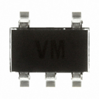
TSV911ILT STMicroelectronics, TSV911ILT Datasheet - Page 2

TSV911ILT
Manufacturer Part Number
TSV911ILT
Description
IC OPAMP RRIO SGL 8MHZ SOT23-5
Manufacturer
STMicroelectronics
Datasheet
1.TSV911ILT.pdf
(20 pages)
Specifications of TSV911ILT
Amplifier Type
General Purpose
Number Of Circuits
1
Output Type
Rail-to-Rail
Slew Rate
4.5 V/µs
Gain Bandwidth Product
8MHz
Current - Input Bias
1pA
Voltage - Input Offset
100µV
Current - Supply
820µA
Current - Output / Channel
35mA
Voltage - Supply, Single/dual (±)
2.5 V ~ 5.5 V
Operating Temperature
-40°C ~ 125°C
Mounting Type
Surface Mount
Package / Case
SOT-23-5, SC-74A, SOT-25
Number Of Channels
1
Common Mode Rejection Ratio (min)
62 dB
Input Offset Voltage
4.5 mV
Input Bias Current (max)
100 pA
Operating Supply Voltage
2.5 V to 5.5 V
Supply Current
1.1 mA
Maximum Operating Temperature
+ 125 C
Minimum Operating Temperature
- 40 C
Mounting Style
SMD/SMT
Shutdown
No
Supply Voltage (max)
5.5 V
Supply Voltage (min)
2.5 V
Voltage Gain Db
91 dB
Lead Free Status / RoHS Status
Lead free / RoHS Compliant
-3db Bandwidth
-
Lead Free Status / Rohs Status
Lead free / RoHS Compliant
Other names
497-6000-2
Available stocks
Company
Part Number
Manufacturer
Quantity
Price
Part Number:
TSV911ILT
Manufacturer:
ST
Quantity:
20 000
Absolute maximum ratings and operating conditions
1
2/20
Absolute maximum ratings and operating conditions
Table 2.
1. All voltage values, except differential voltage, are with respect to network ground terminal.
2. Differential voltages are the non-inverting input terminal with respect to the inverting input terminal.
3. V
4. Input current must be limited by a resistor in series with the inputs.
5. Short-circuits can cause excessive heating and destructive dissipation.
6. R
7. Human body model: a 100 pF capacitor is charged to the specified voltage, then discharged through a
8. Machine model: a 200 pF capacitor is charged to the specified voltage, then discharged directly between
9. Charged device model: all pins and the package are charged together to the specified voltage and then
Symbol
1.5kΩ resistor between two pins of the device. This is done for all couples of connected pin combinations
while the other pins are floating.
two pins of the device with no external series resistor (internal resistor < 5 Ω). This is done for all couples of
connected pin combinations while the other pins are floating.
discharged directly to the ground through only one pin. This is done for all pins.
R
R
ESD
V
T
V
V
CC
th
I
T
thja
CC
stg
thjc
in
id
in
j
are typical values.
-V
in
must not exceed 6 V.
Supply voltage
Differential input voltage
Input voltage
Input current
Storage temperature
Thermal resistance junction to ambient
Thermal resistance junction to case
Maximum junction temperature
HBM: human body model
MM: machine model
CDM: charged device model
Latch-up immunity
Absolute maximum ratings
SOT23-5
SO-8
MiniSO-8
SO-14
TSSOP14
SOT23-5
SO-8
MiniSO-8
SO-14
TSSOP14
SOT23-5, SO-8, MiniSO-8
TSSOP14
SO-14
(4)
(3)
(1)
Doc ID 12584 Rev 7
(8)
Parameter
(2)
(7)
(9)
(5) (6)
(5) (6)
V
CC-
-0.2 to V
-65 to +150
Value
±V
1500
250
125
190
103
100
150
400
750
500
200
10
81
40
39
31
32
6
5
CC
CC+
+0.2
TSV91x
°C/W
°C/W
Unit
mA
mA
kV
°C
°C
V
V
V
V
V


