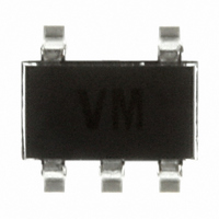
TSH70CLT STMicroelectronics, TSH70CLT Datasheet - Page 21

TSH70CLT
Manufacturer Part Number
TSH70CLT
Description
IC OP AMP SGL LP WIDE SOT23-5
Manufacturer
STMicroelectronics
Datasheet
1.TSH73CPT.pdf
(33 pages)
Specifications of TSH70CLT
Amplifier Type
General Purpose
Number Of Circuits
1
Output Type
Rail-to-Rail
Slew Rate
118 V/µs
Gain Bandwidth Product
65MHz
-3db Bandwidth
100MHz
Current - Input Bias
6µA
Voltage - Input Offset
800µV
Current - Supply
9.8mA
Current - Output / Channel
55mA
Voltage - Supply, Single/dual (±)
3 V ~ 12 V, ±1.5 V ~ 6 V
Operating Temperature
0°C ~ 70°C
Mounting Type
Surface Mount
Package / Case
SOT-23-5, SC-74A, SOT-25
Number Of Channels
1
Common Mode Rejection Ratio (min)
72 dB
Input Offset Voltage
10 mV
Input Bias Current (max)
15 uA
Operating Supply Voltage
5 V, 9 V
Supply Current
10.5 mA
Maximum Operating Temperature
+ 70 C
Minimum Operating Temperature
0 C
Dual Supply Voltage
+/- 3 V, +/- 5 V
Maximum Dual Supply Voltage
+/- 6 V
Minimum Dual Supply Voltage
+/- 1.5 V
Mounting Style
SMD/SMT
Shutdown
No
Supply Voltage (max)
12 V
Supply Voltage (min)
3 V
Voltage Gain Db
84 dB
Lead Free Status / RoHS Status
Lead free / RoHS Compliant
Other names
497-8154-2
TSH70CLT
TSH70CLT
Available stocks
Company
Part Number
Manufacturer
Quantity
Price
Part Number:
TSH70CLT
Manufacturer:
ST
Quantity:
20 000
TSH70,71,72,73,74,75
5
5.1
5.2
Testing Conditions
Layout precautions
To use the TSH7X circuits in the best manner at high frequencies, some precautions have to
be taken for power supplies:
●
●
●
●
●
Maximum input level
Figure 47. CCIR330 video line
The input level must not exceed the following values:
●
●
– First of all, the implementation of a proper ground plane in both sides of the PCB is
– Power supply bypass capacitors (4.7uF and ceramic 100pF) should be placed as
Proper termination of all inputs and outputs must be in accordance with output
termination resistors; in this way, the amplifier load will be resistive only, and the
stability of the amplifier will be improved.
All leads must be wide and as short as possible (especially for op-amp inputs and
outputs) in order to decrease parasitic capacitance and inductance.
For lower gain applications, care should be taken to avoid large feedback resistance
(>1k Ω ) in order to reduce the time constant of parasitic capacitances.
Choose component sizes as small as possible (SMD).
Finally, on output, the load capacitance must be negligible to maintain good stability.
You can put a serial resistance as close as possible to the output pin to minimize
capacitance.
negative peak: must be greater than -V
positive peak value: must be lower than +V
mandatory for high speed circuit applications to provide low inductance and low
resistance common return.
close as possible to the IC pins in order to improve high frequency bypassing and
reduce harmonic distortion. The power supply capacitors must be incorporated for
both the negative and the positive pins.
CC
+400mV.
CC
-400mV.
Testing Conditions
21/33


