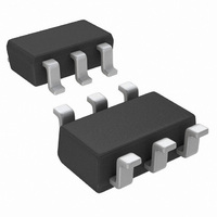
LMV118MF/NOPB National Semiconductor, LMV118MF/NOPB Datasheet - Page 4

LMV118MF/NOPB
Manufacturer Part Number
LMV118MF/NOPB
Description
IC OPAMP SGL R-R SHTDOWN SOT23-6
Manufacturer
National Semiconductor
Datasheet
1.LMV118MFNOPB.pdf
(14 pages)
Specifications of LMV118MF/NOPB
Amplifier Type
Voltage Feedback
Number Of Circuits
1
Output Type
Push-Pull, Rail-to-Rail
Slew Rate
35 V/µs
-3db Bandwidth
45MHz
Current - Input Bias
400nA
Voltage - Input Offset
1000µV
Current - Supply
600µA
Current - Output / Channel
20mA
Voltage - Supply, Single/dual (±)
2.5 V ~ 12 V, ±1.25 V ~ 6 V
Operating Temperature
-40°C ~ 85°C
Mounting Type
Surface Mount
Package / Case
SOT-23-6
Lead Free Status / RoHS Status
Lead free / RoHS Compliant
Gain Bandwidth Product
-
Other names
LMV118MF
LMV118MFTR
LMV118MFTR
Available stocks
Company
Part Number
Manufacturer
Quantity
Price
Company:
Part Number:
LMV118MF/NOPB
Manufacturer:
National Semiconductor
Quantity:
34 858
www.national.com
V
TC V
I
I
CMRR
PSRR
R
C
CMVR
A
V
I
I
I
SR
BW
e
i
t
t
TH
I
n
B
OS
SC
OUT
S
on
off
SD
n
Symbol
OS
VOL
O
IN
IN
±5V Electrical Characteristics
Unless otherwise specified, all limits guaranteed for at T
1kΩ to V
Note 1: Absolute Maximum Ratings indicate limits beyond which damage to the device may occur. Operating Ratings indicate conditions for which the device is
intended to be functional, but specific performance is not guaranteed. For guaranteed specifications and the test conditions, see the Electrical Characteristics.
Note 2: Human body model, 1.5kΩ in series with 100pF.
Note 3: Applies to both single-supply and split-supply operation. Continuous short circuit operation at elevated ambient temperature can result in exceeding the
maximum allowed junction temperature of 150°C.
Note 4: The maximum power dissipation is a function of T
P
Note 5: Typical values represent the most likely parametric norm.
Note 6: All limits are guaranteed by testing or statistical analysis.
Note 7: Positive current corresponds to current flowing into the device.
SD
D
= (T
OS
J(MAX)
+
/2. Boldface limits apply at the temperature extremes.
Input Offset Voltage
Input Offset Average Drift
Input Bias Current
Input Offset Current
Common Mode Rejection Ratio
Power Supply Rejection Ratio
Common Mode Input Resistance
Common Mode Input
Capacitance
Input Common-Mode Voltage
Range
Large Signal Voltage Gain
Output Swing High
Output Swing Low
Output Short Circuit Current
Output Current
Supply Current
Slew Rate
−3dB BW
Input -Referred Voltage Noise
Input-Referred Current Noise
Turn-on Time (LMV118)
Turn-off Time (LMV118)
Shut-down Threshold (LMV118) I
Shutdown Pin Input Current
(LMV118)
- T
A
)/ θ
JA
. All numbers apply for packages soldered directly onto a PC board.
Parameter
(Note
8)
−5V
(Note
(Note
V
V
CMRR
V
R
R
R
R
Sourcing to 0V
V
Sinking to 0V
V
V
Normal Operation
Shut-down Mode (LMV118)
A
A
f = 100kHz
f = 1kHz
f = 100kHz
f = 1kHz
(Note
S
CM
+
O
ID
ID
OUT
V
V
L
L
L
L
≤
J(MAX)
= 5V to 6V or V
= 1kΩ
= 10kΩ
= 1kΩ
= 10kΩ
= +1, V
= +1, V
= −2V to 2V
= 200mV
= −200mV
Stepped from −5V to 3.5V
50μA
≤
= 0.5V from rails
12)
7)
7)
V
, θ
≥
CM
JA
50dB
, and T
O
OUT
J
≤
= 1V
= 25°C, V
(Note
Conditions
1.7V
= 200mV
(Note
A
. The maximum allowable power dissipation at any ambient temperature is
PP
−
4
10)
= −5V to −6V
10)
+
PP
= 5V, V
−
= −5V, V
(Note
CM
−4.70
−2.0
−2.2
−5.3
−5.1
4.70
Min
78
72
74
71
40
40
= V
6)
O
= 0V, and R
(Note
−0.40
−4.93
−4.98
4.92
4.97
0.75
1.20
4.25
Typ
±20
−20
104
600
200
700
±1
±5
95
85
57
54
15
35
45
40
60
3
3
2
5)
F
= 2kΩ, and R
(Note
Max
4.60
500
900
4.0
±5
±6
50
6)
nV/
pA/
L
Units
μV/C
V/μs
MHz
MΩ
=
mV
mV
mA
mA
μA
nA
dB
dB
pF
dB
μA
μA
ns
ns
V
V
V


