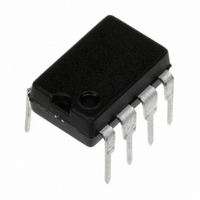
LMC6482IN/NOPB National Semiconductor, LMC6482IN/NOPB Datasheet - Page 17

LMC6482IN/NOPB
Manufacturer Part Number
LMC6482IN/NOPB
Description
IC OP AMP DUAL CMOS R-R 8-DIP
Manufacturer
National Semiconductor
Specifications of LMC6482IN/NOPB
Amplifier Type
General Purpose
Number Of Circuits
2
Output Type
Rail-to-Rail
Slew Rate
1.3 V/µs
Gain Bandwidth Product
1.5MHz
Current - Input Bias
0.02pA
Voltage - Input Offset
110µV
Current - Supply
1.3mA
Current - Output / Channel
30mA
Voltage - Supply, Single/dual (±)
3 V ~ 15.5 V, ±1.5 V ~ 7.75 V
Operating Temperature
-40°C ~ 85°C
Mounting Type
Through Hole
Package / Case
8-DIP (0.300", 7.62mm)
Bandwidth
1.5 MHz
Channel Separation
150
Common Mode Rejection Ratio
82
Current, Input Bias
0.02 pA
Current, Input Offset
0.01 pA
Current, Output
30 mA
Current, Supply
1.3 mA
Harmonic Distortion
0.01 %
Impedance, Thermal
90 °C/W
Number Of Amplifiers
Dual
Package Type
MDIP-8
Resistance, Input
10 Teraohms
Temperature, Operating, Range
-40 to +85 °C
Voltage, Gain
666 V/mV
Voltage, Input
3 to 15.5 V
Voltage, Noise
37 nV/sqrt Hz
Voltage, Offset
0.11 mV
Voltage, Output, High
14.7 V
Voltage, Output, Low
0.16 V
Voltage, Supply
5 V
Lead Free Status / RoHS Status
Lead free / RoHS Compliant
-3db Bandwidth
-
Lead Free Status / Rohs Status
RoHS Compliant part
Electrostatic Device
Other names
*LMC6482IN
*LMC6482IN/NOPB
LMC6482IN
*LMC6482IN/NOPB
LMC6482IN
Application Information
7.0 OFFSET VOLTAGE ADJUSTMENT
Offset voltage adjustment circuits are illustrated in Figure 12
Figure 13. Large value resistances and potentiometers are
used to reduce power consumption while providing typically
configurations with V
±
2.5mV of adjustment range, referred to the input, for both
FIGURE 13. Non-Inverting Configuration
FIGURE 12. Inverting Configuration
Offset Voltage Adjustment
Offset Voltage Adjustment
S
=
±
5V.
(Continued)
01171325
01171326
17
8.0 UPGRADING APPLICATIONS
The LMC6484 quads and LMC6482 duals have industry
standard pin outs to retrofit existing applications. System
performance can be greatly increased by the LMC6482’s
features. The key benefit of designing in the LMC6482 is
increased linear signal range. Most op-amps have limited
input common mode ranges. Signals that exceed this range
generate a non-linear output response that persists long
after the input signal returns to the common mode range.
Linear signal range is vital in applications such as filters
where signal peaking can exceed input common mode
ranges resulting in output phase inverison or severe distor-
tion.
9.0 DATA ACQUISITION SYSTEMS
Low power, single supply data acquisition system solutions
are provided by buffering the ADC12038 with the LMC6482
(Figure 14). Capable of using the full supply range, the
LMC6482 does not require input signals to be scaled down
to meet limited common mode voltage ranges. The
LMC4282 CMRR of 82dB maintains integral linearity of a
12-bit data acquisition system to
rail input amplifiers with only 50dB of CMRR will degrade the
accuracy of the data acquisition system to only 8 bits.
±
0.325 LSB. Other rail-to-
www.national.com


