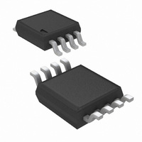
LMH6504MM/NOPB National Semiconductor, LMH6504MM/NOPB Datasheet - Page 17

LMH6504MM/NOPB
Manufacturer Part Number
LMH6504MM/NOPB
Description
IC AMP VAR GAIN LOW POWER 8MSOP
Manufacturer
National Semiconductor
Series
LMH®r
Type
Variable Gain Amplifierr
Datasheet
1.LMH6504MMNOPB.pdf
(19 pages)
Specifications of LMH6504MM/NOPB
Amplifier Type
Variable Gain
Number Of Circuits
1
Slew Rate
1500 V/µs
-3db Bandwidth
150MHz
Current - Input Bias
1.4µA
Current - Supply
11mA
Current - Output / Channel
80mA
Voltage - Supply, Single/dual (±)
7 V ~ 12 V, ±3.5 V ~ 6 V
Operating Temperature
-40°C ~ 85°C
Mounting Type
Surface Mount
Package / Case
8-MSOP, Micro8™, 8-uMAX, 8-uSOP,
Number Of Channels
1
Number Of Elements
1
Power Supply Requirement
Dual
Input Resistance
7MOhm
Input Bias Current
3.5uA
Single Supply Voltage (typ)
Not RequiredV
Dual Supply Voltage (typ)
±5V
Power Supply Rejection Ratio
65dB
Rail/rail I/o Type
No
Single Supply Voltage (min)
Not RequiredV
Single Supply Voltage (max)
Not RequiredV
Dual Supply Voltage (min)
±3.5V
Dual Supply Voltage (max)
±6V
Operating Temp Range
-40C to 85C
Operating Temperature Classification
Industrial
Mounting
Surface Mount
Pin Count
8
Package Type
MSOP
Lead Free Status / RoHS Status
Lead free / RoHS Compliant
Output Type
-
Gain Bandwidth Product
-
Voltage - Input Offset
-
Lead Free Status / Rohs Status
Compliant
Other names
LMH6504MM
LMH6504MMTR
LMH6504MMTR
Available stocks
Company
Part Number
Manufacturer
Quantity
Price
Application Information
CIRCUIT LAYOUT CONSIDERATIONS & EVALUATION
BOARD
A good high frequency PCB layout including ground plane
construction and power supply bypassing close to the pack-
age are critical to achieving full performance. The amplifier is
sensitive to stray capacitance to ground at the I
keep node trace area small. Shunt capacitance across the
feedback resistor should not be used to compensate for this
effect. Capacitance to ground should be minimized by re-
moving the ground plane from under the body of R
sitic or load capacitance directly on the output (pin 6) de-
grades phase margin leading to frequency response
peaking.
The LMH6504 is fully stable when driving a 100Ω load. With
reduced load (e.g. 1k.) there is a possibility of instability at
very high frequencies beyond 400 MHz especially with a
capacitive load. When the LMH6504 is connected to a light
load as such, it is recommended to add a snubber network to
FIGURE 9. Automatic Gain Control Circuit #2
(Continued)
-
input (pin 7);
G
. Para-
17
the output (e.g. 100Ω and 39 pF in series tied between the
LMH6504 output and ground). C
the output by placing a small resistor in series with the output
(pin 6).
Component parasitics also influence high frequency results.
Therefore it is recommended to use metal film resistors such
as RN55D or leadless components such as surface mount
devices. High profile sockets are not recommended.
National Semiconductor suggests the following evaluation
board as a guide for high frequency layout and as an aid in
device testing and characterization:
The evaluation board is shipped when a device sample
request is placed with National Semiconductor.
Device
LMH6504
Package
SOIC
L
can also be isolated from
Evaluation Board
Part Number
CLC730066
20084360
www.national.com


