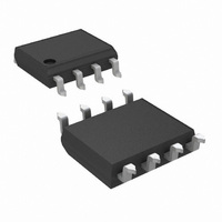
LM7171AIM/NOPB National Semiconductor, LM7171AIM/NOPB Datasheet - Page 17

LM7171AIM/NOPB
Manufacturer Part Number
LM7171AIM/NOPB
Description
IC AMP VERY HI SPD V FDBK 8-SOIC
Manufacturer
National Semiconductor
Series
VIP™ IIIr
Type
Voltage Feedback Amplifierr
Datasheet
1.LM7171BINNOPB.pdf
(20 pages)
Specifications of LM7171AIM/NOPB
Amplifier Type
Voltage Feedback
Number Of Circuits
1
Slew Rate
4100 V/µs
Gain Bandwidth Product
200MHz
-3db Bandwidth
220MHz
Current - Input Bias
2.7µA
Voltage - Input Offset
200µV
Current - Supply
6.5mA
Current - Output / Channel
118mA
Voltage - Supply, Single/dual (±)
5.5 V ~ 36 V, ±2.75 V ~ 18 V
Operating Temperature
-40°C ~ 85°C
Mounting Type
Surface Mount
Package / Case
8-SOIC (3.9mm Width)
Rail/rail I/o Type
No
Number Of Elements
1
Unity Gain Bandwidth Product
125MHz
Common Mode Rejection Ratio
80dB
Input Offset Voltage
1.5mV
Input Bias Current
10uA
Single Supply Voltage (typ)
9/12/15/18/24/28V
Voltage Gain In Db
78dB
Power Supply Rejection Ratio
85dB
Power Supply Requirement
Single/Dual
Shut Down Feature
No
Single Supply Voltage (min)
5.5V
Single Supply Voltage (max)
36V
Dual Supply Voltage (min)
±2.75V
Dual Supply Voltage (max)
±18V
Technology
BiCOM
Operating Temp Range
-40C to 85C
Operating Temperature Classification
Industrial
Mounting
Surface Mount
Pin Count
8
Package Type
SOIC N
Lead Free Status / RoHS Status
Lead free / RoHS Compliant
Output Type
-
Lead Free Status / Rohs Status
RoHS Compliant part
Electrostatic Device
Other names
*LM7171AIM
*LM7171AIM/NOPB
LM7171AIM
*LM7171AIM/NOPB
LM7171AIM
Application Notes
ally by placing 0.01 µF ceramic capacitors directly to power
supply pins and 2.2 µF tantalum capacitors close to the
power supply pins.
TERMINATION
In high frequency applications, reflections occur if signals
are not properly terminated. Figure 3 shows a properly ter-
minated signal while Figure 4 shows an improperly termi-
nated signal.
FIGURE 4. Improperly Terminated Signal
FIGURE 3. Properly Terminated Signal
FIGURE 2. Power Supply Bypassing
(Continued)
01238511
01238517
01238518
17
To minimize reflection, coaxial cable with matching charac-
teristic impedance to the signal source should be used. The
other end of the cable should be terminated with the same
value terminator or resistor. For the commonly used cables,
RG59 has 75Ω characteristic impedance, and RG58 has
50Ω characteristic impedance.
DRIVING CAPACITIVE LOADS
Amplifiers driving capacitive loads can oscillate or have ring-
ing at the output. To eliminate oscillation or reduce ringing,
an isolation resistor can be placed as shown below in Figure
5. The combination of the isolation resistor and the load
capacitor forms a pole to increase stability by adding more
phase margin to the overall system. The desired perfor-
mance depends on the value of the isolation resistor; the
bigger the isolation resistor, the more damped the pulse
response becomes. For LM7171, a 50Ω isolation resistor is
recommended for initial evaluation. Figure 6 shows the
LM7171 driving a 150 pF load with the 50Ω isolation resistor.
POWER DISSIPATION
The maximum power allowed to dissipate in a device is
defined as:
Where
For example, for the LM7171 in a SO-8 package, the maxi-
mum power dissipation at 25˚C ambient temperature is
730 mW.
PD
T
T
θ
JA
J(max)
A
FIGURE 6. The LM7171 Driving a 150 pF Load
is the power dissipation in a device
is the maximum junction temperature
is the ambient temperature
is the thermal resistance of a particular package
FIGURE 5. Isolation Resistor Used
with a 50Ω Isolation Resistor
to Drive Capacitive Load
P
D
= (T
J(MAX)
− T
A
)/θ
JA
01238513
www.national.com
01238512


