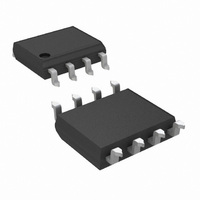
LMH6702MA/NOPB National Semiconductor, LMH6702MA/NOPB Datasheet - Page 10

LMH6702MA/NOPB
Manufacturer Part Number
LMH6702MA/NOPB
Description
IC OPAMP LOW DISTOR 720MHZ 8SOIC
Manufacturer
National Semiconductor
Series
PowerWise®r
Datasheet
1.LMH6702MFNOPB.pdf
(13 pages)
Specifications of LMH6702MA/NOPB
Amplifier Type
Current Feedback
Number Of Circuits
1
Slew Rate
3100 V/µs
-3db Bandwidth
1.7GHz
Current - Input Bias
6µA
Voltage - Input Offset
1000µV
Current - Supply
12.5mA
Current - Output / Channel
80mA
Voltage - Supply, Single/dual (±)
10 V ~ 12 V, ±5 V ~ 6 V
Operating Temperature
-40°C ~ 85°C
Mounting Type
Surface Mount
Package / Case
8-SOIC (3.9mm Width)
Number Of Channels
1
Common Mode Rejection Ratio (min)
45 dB
Input Offset Voltage
4.5 mV at +/- 5 V
Supply Current
16.1 mA at +/- 5 V
Maximum Operating Temperature
+ 85 C
Maximum Dual Supply Voltage
+/- 6 V
Minimum Operating Temperature
- 40 C
For Use With
LMH730227 - BOARD EVALUATION FOR SOIC PKGLMH730165 - BOARD EVALUATIONLMH730216 - BOARD EVAL HS MONO AMP SOT23
Lead Free Status / RoHS Status
Lead free / RoHS Compliant
Output Type
-
Gain Bandwidth Product
-
Lead Free Status / Rohs Status
Details
Other names
*LMH6702MA
LMH6702MA
LMH6702MA
www.national.com
Application Section
The LMH6702 data sheet shows both SOT23 and SOIC data
in the Electrical Characteristic section to aid in selecting the
right package. The Typical Performance Characteristics sec-
tion shows SOIC package plots only.
2-TONE 3
The 2-tone, 3rd order spurious plot shows a relatively con-
stant difference between the test power level and the spuri-
ous level with the difference depending on frequency. The
LMH6702 does not show an intercept type performance,
(where the relative spurious levels change at a 2X rate vs.
the test tone powers), due to an internal full power bandwidth
enhancement circuit that boosts the performance as the
output swing increases while dissipating negligible quiescent
power under low output power conditions. This feature en-
hances the distortion performance and full power bandwidth
to match that of much higher quiescent supply current parts.
FIGURE 4. SOIC and SOT23-5 Packages Distortion
rd
ORDER INTERMODULATION
Terms Compared
(Continued)
20039023
10
CAPACITIVE LOAD DRIVE
Figure 5 shows a typical application using the LMH6702 to
drive an ADC.
The series resistor, R
ADC input is critical to achieving best system performance.
This load capacitance, if applied directly to the output pin,
can quickly lead to unacceptable levels of ringing in the
pulse response. The plot of "R
the Typical Performance Characteristics section is an excel-
lent starting point for selecting R
plot minimizes the step settling time into a fixed discrete
capacitive load with the output driving a very light resistive
load (1kΩ). Sensitivity to capacitive loading is greatly re-
duced once the output is loaded more heavily. Therefore, for
cases where the output is heavily loaded, R
reduced. The exact value may best be determined experi-
mentally for these cases.
In applications where the LMH6702 is replacing the CLC409,
care must be taken when the device is lightly loaded and
some capacitance is present at the output. Due to the much
higher frequency response of the LMH6702 compared to the
CLC409, there could be increased susceptibility to low value
output capacitance (parasitic or inherent to the board layout
or otherwise being part of the output load). As already men-
tioned, this susceptibility is most noticeable when the
LMH6702’s resistive load is light. Parasitic capacitance can
be minimized by careful lay out. Addition of an output snub-
ber R-C network will also help by increasing the high fre-
quency resistive loading.
Referring back to Figure 5, it must be noted that several
additional constraints should be considered in driving the
capacitive input of an ADC. There is an option to increase
R
band-limiting purposes. Increasing R
can induce an unacceptably large input glitch due to switch-
ing transients coupling through from the "convert" signal.
Also, C
This input impedance non-linearity will induce distortion
terms that will increase as R
adjustments up or down from the recommended R
should therefore be attempted in optimizing system perfor-
mance.
S
, band-limiting at the ADC input for either noise or Nyquist
IN
is oftentimes a voltage dependent capacitance.
FIGURE 5. Input Amplifier to ADC
S
, between the amplifier output and the
S
S
and Settling Time vs. C
S
. The value derived in that
is increased. Only slight
S
too much, however,
S
value may be
20039029
S
value
L
" in


