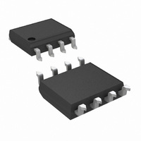
LMH6504MA/NOPB National Semiconductor, LMH6504MA/NOPB Datasheet - Page 16

LMH6504MA/NOPB
Manufacturer Part Number
LMH6504MA/NOPB
Description
IC AMP VARIABLE GAIN 8-SOIC
Manufacturer
National Semiconductor
Series
LMH®r
Datasheet
1.LMH6504MMNOPB.pdf
(19 pages)
Specifications of LMH6504MA/NOPB
Amplifier Type
Variable Gain
Number Of Circuits
1
Slew Rate
1500 V/µs
-3db Bandwidth
150MHz
Current - Input Bias
1.4µA
Current - Supply
11mA
Current - Output / Channel
80mA
Voltage - Supply, Single/dual (±)
7 V ~ 12 V, ±3.5 V ~ 6 V
Operating Temperature
-40°C ~ 85°C
Mounting Type
Surface Mount
Package / Case
8-SOIC (3.9mm Width)
Lead Free Status / RoHS Status
Lead free / RoHS Compliant
Output Type
-
Gain Bandwidth Product
-
Voltage - Input Offset
-
Other names
*LMH6504MA
*LMH6504MA/NOPB
LMH6504MA
*LMH6504MA/NOPB
LMH6504MA
www.national.com
Application Information
Signal frequencies must not reach the gain control port of the
LMH6504, or the output signal will be distorted (modulated
by itself). A fast settling AGC needs additional filtering be-
yond the integrator stage to block signal frequencies. This is
provided in Figure 8 by a simple R-C filter (R
better distortion performance can be achieved with a more
complex filter. These filters should be scaled with the input
signal frequency. Loops with slower response time (longer
integration time constants) may not need the R
Checking the loop stability can be done by monitoring the V
voltage while applying a step change in input signal ampli-
tude. Changing the input signal amplitude can be easily
done with an arbitrary waveform generator.
AUTOMATIC GAIN CONTROL (AGC) #2
Figure 9 illustrates an automatic gain control circuit that
employs two LMH6504’s. In this circuit, U1 receives the input
signal and produces an output signal of constant amplitude.
FIGURE 8. Automatic Gain Control Circuit #1
(Continued)
10
10
– C
and C
3
filter.
3
);
G
16
U2 is configured to provide negative feedback. U2 generates
a rectified gain control signal that works against an adjust-
able bias level which may be set by the potentiometer and
R
ant gain control signal is applied to the U1 gain control input
V
arbitrary level less than the maximum output specification of
the amplifier. Rectification is accomplished in U2 by driving
both the amplifier input and the gain control input with the U1
output signal. The voltage divider that is formed by R
R
G
B
2
, sets the rectifier gain.
. C
. The bias adjustment allows the U1 output to be set at an
I
integrates the bias and negative feedback. The result-
20084359
1
and


