LM6144BIM/NOPB National Semiconductor, LM6144BIM/NOPB Datasheet - Page 5
LM6144BIM/NOPB
Manufacturer Part Number
LM6144BIM/NOPB
Description
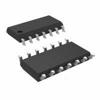
IC OP AMP QUAD R-R HS LP 14-SOIC
Manufacturer
National Semiconductor
Datasheet
1.LM6142BIMX.pdf
(16 pages)
Specifications of LM6144BIM/NOPB
Amplifier Type
General Purpose
Number Of Circuits
4
Output Type
Rail-to-Rail
Slew Rate
25 V/µs
Gain Bandwidth Product
9MHz
Current - Input Bias
174nA
Voltage - Input Offset
1300µV
Current - Supply
750µA
Current - Output / Channel
22mA
Voltage - Supply, Single/dual (±)
1.8 V ~ 24 V, ±0.9 V ~ 12 V
Operating Temperature
-40°C ~ 85°C
Mounting Type
Surface Mount
Package / Case
14-SOIC (3.9mm Width), 14-SOL
Lead Free Status / RoHS Status
Lead free / RoHS Compliant
-3db Bandwidth
-
Other names
*LM6144BIM
*LM6144BIM/NOPB
LM6144BIM
*LM6144BIM/NOPB
LM6144BIM


V
I
I
R
CMRR
PSRR
V
A
V
I
GBW
B
OS
S
24V Electrical Characteristics
Unless Otherwise Specified, All Limits Guaranteed for T
V
OS
IN
CM
V
O
Note 1: Absolute Maximum Ratings indicate limits beyond which damage to the device may occur. Operating Ratings indicate conditions for which the device is
intended to be functional, but specific performance is not guaranteed. For guaranteed specifications and the test conditions, see the Electrical Charactenstics.
Note 2: Human body model, 1.5kΩ in series with 100pF.
Note 3: Applies to both single-supply and split-supply operation. Continuous short circuit operation at elevated ambient temperature can result in exceeding the
maximum allowed junction temperature of 150˚C.
Note 4: The maximum power dissipation is a function of T
(T
Note 5: Typical values represent the most likely parametric norm.
Note 6: All limits are guaranteed by testing or statistical analysis.
Note 7: For guaranteed military specifications see military datasheet MNLM6142AM-X.
Note 8: Electrical Table values apply only for factory testing conditions at the temperature indicated. Factory testing conditions result in very limited self-heating of
the device such that T
T
Symbol
A
+
J(MAX)
.
/2. Boldface limits apply at the temperature extreme
− T
A
)/θ
JA
Input Offset Voltage
Input Bias Current
Input Offset Current
Input Resistance
Common Mode
Rejection Ratio
Power Supply
Rejection Ratio
Input Common-Mode
Voltage Range
Large Signal
Voltage Gain
Output Swing
Supply Current
Gain-Bandwidth Product
. All numbers apply for packages soldered directly into a PC board.
J
= T
A
Parameter
. No guarantee of parametric performance is indicated in the electrical tables under conditions of the internal self heating where T
0V ≤ V
0V ≤ V
0V ≤ V
R
R
Per Amplifier
f = 50 kHz
L
L
J(MAX)
= 10k
= 10 kΩ
Conditions
(Note 8)
CM
CM
CM
, θ
JA
≤ 23V
≤ 24V
≤ 24V
, and T
A
= 25˚C, V
A
. The maximum allowable power dissipation at any ambient temperature is P
5
+
= 24V, V
(Note 5)
−0.25
24.25
23.85
0.07
Typ
174
288
114
100
500
750
1.3
87
18
5
−
= 0V, V
LM6144AI
LM6142AI
(Note 6)
CM
0.185
23.81
23.62
Limit
1100
1150
0.15
4.8
24
2
0
= V
O
= V
+
/2 and R
LM6144BI
LM6142BI
(Note 6)
0.185
23.81
23.62
Limit
1100
1150
0.15
3.8
4.8
24
0
L
>
1 MΩ to
www.national.com
V max
V min
Units
V/mV
MHz
max
max
max
max
max
MΩ
min
min
min
mV
nA
nA
dB
µA
V
V
D
J
>
=
Related parts for LM6144BIM/NOPB
Image
Part Number
Description
Manufacturer
Datasheet
Request
R

Part Number:
Description:
IC, OP-AMP, 17MHZ, 25V/µs, SOIC-14
Manufacturer:
National Semiconductor
Datasheet:

Part Number:
Description:
National Semiconductor [8-Bit D/A Converter]
Manufacturer:
National Semiconductor
Datasheet:
Part Number:
Description:
National Semiconductor [Media Coprocessor]
Manufacturer:
National Semiconductor
Datasheet:
Part Number:
Description:
Digitally Controlled Tone and Volume Circuit with Stereo Audio Power Amplifier, Microphone Preamp Stage and National 3D Sound
Manufacturer:
National Semiconductor
Datasheet:
Part Number:
Description:
Digitally Controlled Tone and Volume Circuit with Stereo Audio Power Amplifier, Microphone Preamp Stage and National 3D Sound
Manufacturer:
National Semiconductor
Datasheet:
Part Number:
Description:
AC97 Rev 2 Codec with Sample Rate Conversion and National 3D Sound
Manufacturer:
National Semiconductor
Part Number:
Description:
Manufacturer:
National Semiconductor
Datasheet:
Part Number:
Description:
Manufacturer:
National Semiconductor
Datasheet:
Part Number:
Description:
General Purpose, Low Voltage, Low Power, Rail-to-Rail Output Operational Amplifiers
Manufacturer:
National Semiconductor
Datasheet:
Part Number:
Description:
8-bit 20 MSPS flash A/D converter.
Manufacturer:
National Semiconductor
Datasheet:
Part Number:
Description:
Low Noise Quad Operational Amplifier
Manufacturer:
National Semiconductor
Datasheet:
Part Number:
Description:
Quad Differential Line Receivers
Manufacturer:
National Semiconductor
Datasheet:
Part Number:
Description:
Quad High Speed Trapezoidal? Bus Transceiver
Manufacturer:
National Semiconductor
Datasheet:
Part Number:
Description:
Dual Line Receiver
Manufacturer:
National Semiconductor
Datasheet: