LM2902NG ON Semiconductor, LM2902NG Datasheet - Page 13
LM2902NG
Manufacturer Part Number
LM2902NG
Description
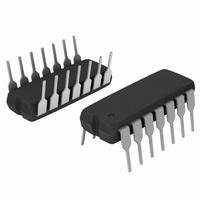
IC OPAMP QUAD SGL SUPPLY 14DIP
Manufacturer
ON Semiconductor
Specifications of LM2902NG
Amplifier Type
General Purpose
Number Of Circuits
4
Slew Rate
0.6 V/µs
Gain Bandwidth Product
1MHz
Current - Input Bias
90nA
Voltage - Input Offset
2000µV
Current - Supply
1.4mA
Current - Output / Channel
40mA
Voltage - Supply, Single/dual (±)
3 V ~ 32 V, ±1.5 V ~ 16 V
Operating Temperature
-40°C ~ 105°C
Mounting Type
Through Hole
Package / Case
14-DIP (0.300", 7.62mm)
Number Of Channels
4
Common Mode Rejection Ratio (min)
50 dB
Input Voltage Range (max)
Positive Rail - 5.7 V
Input Voltage Range (min)
Negative Rail
Input Offset Voltage
7 mV
Input Bias Current (max)
250 nA
Output Current (typ)
40 mA
Operating Supply Voltage
32 V
Supply Current
1.2 mA
Maximum Operating Temperature
+ 105 C
Minimum Operating Temperature
- 40 C
Dual Supply Voltage
+/- 3 V, +/- 5 V, +/- 9 V
Maximum Dual Supply Voltage
+/- 16 V
Minimum Dual Supply Voltage
+/- 1.5 V
Mounting Style
Through Hole
Shutdown
No
Supply Voltage (max)
32 V
Supply Voltage (min)
3 V
Technology
Bipolar
Voltage Gain Db
100 dB
Bandwidth
1 MHz
Channel Separation
-120
Common Mode Rejection Ratio
70
Current, Input Bias
-500 nA
Current, Input Offset
200 nA
Current, Output
40 mA
Current, Supply
3 mA
Number Of Amplifiers
Quad
Package Type
PDIP-14
Temperature, Operating, Range
-40 to +105 °C
Voltage, Gain
15 V/mV
Voltage, Input
-0.3 to 32 VDC
Voltage, Offset
10 mV
Voltage, Output, High
3.5 V
Voltage, Output, Low
5 mV
Voltage, Supply
3 to 32 VDC
Lead Free Status / RoHS Status
Lead free / RoHS Compliant
Output Type
-
-3db Bandwidth
-
Lead Free Status / Rohs Status
Lead free / RoHS Compliant
Other names
LM2902NGOS


SEATING
PLANE
−T−
14
1
G
−A−
D
14 PL
0.25 (0.010)
M
*For additional information on our Pb−Free strategy and soldering
8
7
details, please download the ON Semiconductor Soldering and
Mounting Techniques Reference Manual, SOLDERRM/D.
−B−
0.58
T
14X
K
B
S
C
P
7 PL
A
S
0.25 (0.010)
PACKAGE DIMENSIONS
SOLDERING FOOTPRINT*
R
http://onsemi.com
1
X 45
CASE 751A−03
_
M
SOIC−14
ISSUE H
M
7.04
7X
B
13
M
DIMENSIONS: MILLIMETERS
J
1.52
14X
F
1.27
PITCH
NOTES:
1. DIMENSIONING AND TOLERANCING PER
2. CONTROLLING DIMENSION: MILLIMETER.
3. DIMENSIONS A AND B DO NOT INCLUDE
4. MAXIMUM MOLD PROTRUSION 0.15 (0.006)
5. DIMENSION D DOES NOT INCLUDE
ANSI Y14.5M, 1982.
MOLD PROTRUSION.
PER SIDE.
DAMBAR PROTRUSION. ALLOWABLE
DAMBAR PROTRUSION SHALL BE 0.127
(0.005) TOTAL IN EXCESS OF THE D
DIMENSION AT MAXIMUM MATERIAL
CONDITION.
DIM
G
M
A
B
C
D
F
J
K
P
R
MILLIMETERS
MIN
8.55
3.80
1.35
0.35
0.40
0.19
0.10
5.80
0.25
1.27 BSC
0
_
MAX
8.75
4.00
1.75
0.49
1.25
0.25
0.25
6.20
0.50
7
_
0.337
0.150
0.054
0.014
0.016
0.008
0.004
0.228
0.010
MIN
0.050 BSC
0
INCHES
_
0.344
0.157
0.068
0.019
0.049
0.009
0.009
0.244
0.019
MAX
7
_
Related parts for LM2902NG
Image
Part Number
Description
Manufacturer
Datasheet
Request
R

Part Number:
Description:
ON Semiconductor [VOLTAGE REGULATOR]
Manufacturer:
ON Semiconductor
Datasheet:
Part Number:
Description:
357-036-542-201 CARDEDGE 36POS DL .156 BLK LOPRO
Manufacturer:
ON Semiconductor
Datasheet:
Part Number:
Description:
357-036-542-201 CARDEDGE 36POS DL .156 BLK LOPRO
Manufacturer:
ON Semiconductor
Datasheet:
Part Number:
Description:
357-036-542-201 CARDEDGE 36POS DL .156 BLK LOPRO
Manufacturer:
ON Semiconductor
Datasheet:
Part Number:
Description:
357-036-542-201 CARDEDGE 36POS DL .156 BLK LOPRO
Manufacturer:
ON Semiconductor
Datasheet:
Part Number:
Description:
357-036-542-201 CARDEDGE 36POS DL .156 BLK LOPRO
Manufacturer:
ON Semiconductor
Datasheet:
Part Number:
Description:
357-036-542-201 CARDEDGE 36POS DL .156 BLK LOPRO
Manufacturer:
ON Semiconductor
Datasheet:
Part Number:
Description:
357-036-542-201 CARDEDGE 36POS DL .156 BLK LOPRO
Manufacturer:
ON Semiconductor
Datasheet:
Part Number:
Description:
357-036-542-201 CARDEDGE 36POS DL .156 BLK LOPRO
Manufacturer:
ON Semiconductor
Datasheet:
Part Number:
Description:
357-036-542-201 CARDEDGE 36POS DL .156 BLK LOPRO
Manufacturer:
ON Semiconductor
Datasheet:
Part Number:
Description:
357-036-542-201 CARDEDGE 36POS DL .156 BLK LOPRO
Manufacturer:
ON Semiconductor
Datasheet:
Part Number:
Description:
Manufacturer:
ON Semiconductor
Datasheet:
Part Number:
Description:
Manufacturer:
ON Semiconductor
Datasheet:
Part Number:
Description:
Manufacturer:
ON Semiconductor
Datasheet: