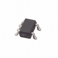
MAX4412EXK+T Maxim Integrated Products, MAX4412EXK+T Datasheet - Page 11

MAX4412EXK+T
Manufacturer Part Number
MAX4412EXK+T
Description
IC OP AMP SGL LP R-R SC70-5
Manufacturer
Maxim Integrated Products
Datasheet
1.MAX4412EUKT.pdf
(16 pages)
Specifications of MAX4412EXK+T
Amplifier Type
Voltage Feedback
Number Of Circuits
1
Output Type
Rail-to-Rail
Slew Rate
140 V/µs
-3db Bandwidth
500MHz
Current - Input Bias
1.6µA
Voltage - Input Offset
400µV
Current - Supply
1.7mA
Current - Output / Channel
75mA
Voltage - Supply, Single/dual (±)
2.7 V ~ 5.5 V
Operating Temperature
-40°C ~ 85°C
Mounting Type
Surface Mount
Package / Case
SC-70-5, SC-88A, SOT-323-5, SOT-353, 5-TSSOP
Number Of Channels
1
Voltage Gain Db
93 dB
Common Mode Rejection Ratio (min)
60 dB
Input Offset Voltage
0.4 mV
Operating Supply Voltage
3 V, 5 V
Maximum Power Dissipation
247 mW
Maximum Operating Temperature
+ 85 C
Mounting Style
SMD/SMT
Minimum Operating Temperature
- 40 C
Lead Free Status / RoHS Status
Lead free / RoHS Compliant
Gain Bandwidth Product
-
Lead Free Status / Rohs Status
Details
Other names
MAX4412EXK+T
MAX4412EXK+TTR
MAX4412EXK+TTR
Input buffer amplifiers can be a source of significant
errors in high-speed analog-to-digital converter (ADC)
applications. The input buffer is usually required to
rapidly charge and discharge the ADC’s input, which is
often capacitive (see Output Capacitive Loading and
Stability ). In addition, since a high-speed ADC’s input
impedance often changes very rapidly during the con-
version cycle, measurement accuracy must be main-
tained using an amplifier with very low output
impedance at high frequencies. The combination of
high speed, fast slew rate, low noise, and a low and
stable distortion overload makes the MAX4412/
MAX4413 ideally suited for use as buffer amplifiers in
high-speed ADC applications.
Low-Cost, Low-Power, Ultra-Small, 3V/5V, 500MHz
Single-Supply Op Amps with Rail-to-Rail Outputs
f
0
=
Q
2
1
=
π
______________________________________________________________________________________
×
C
R
1
1
1
R
×
2
+
C
×
2
R
C
R
1
2
×
2
3
R
+
×
1
2
ADC Input Buffer
C
R
×
1
1
3
R
×
3
C
2
These amplifiers operate from a single +2.7V to +5.5V
power supply. Bypass V
capacitor as close to the pin as possible.
Maxim recommends using microstrip and stripline tech-
niques to obtain full bandwidth. Design the PC board
for a frequency greater than 1GHz to prevent amplifier
performance degradation due to board parasitics.
Avoid large parasitic capacitances at inputs and out-
puts. Whether or not a constant-impedance board is
used, observe the following guidelines:
• Do not use wire-wrap boards due to their high induc-
• Do not use IC sockets because of the increased par-
• Use surface-mount instead of through-hole compo-
• Use a PC board with at least two layers; it should be
• Keep signal lines as short and as straight as possible.
tance.
asitic capacitance and inductance.
nents for better high-frequency performance.
as free from voids as possible.
Do not make 90° turns; round all corners.
Layout and Power-Supply Bypassing
CC
to ground with a 0.1µF
11


