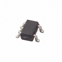
MAX4291EXK+T Maxim Integrated Products, MAX4291EXK+T Datasheet - Page 8

MAX4291EXK+T
Manufacturer Part Number
MAX4291EXK+T
Description
IC OP AMP R-R I/O SC70-5
Manufacturer
Maxim Integrated Products
Datasheet
1.MAX4291EUKT.pdf
(18 pages)
Specifications of MAX4291EXK+T
Amplifier Type
General Purpose
Number Of Circuits
1
Output Type
Rail-to-Rail
Slew Rate
0.2 V/µs
Gain Bandwidth Product
500kHz
Current - Input Bias
15nA
Voltage - Input Offset
400µV
Current - Supply
100µA
Current - Output / Channel
20mA
Voltage - Supply, Single/dual (±)
1.8 V ~ 5.5 V, ±0.9 V ~ 2.75 V
Operating Temperature
-40°C ~ 85°C
Mounting Type
Surface Mount
Package / Case
SC-70-5, SC-88A, SOT-323-5, SOT-353, 5-TSSOP
Number Of Channels
1
Voltage Gain Db
130 dB
Common Mode Rejection Ratio (min)
50 dB
Input Offset Voltage
2.5 mV
Operating Supply Voltage
3 V, 5 V
Maximum Power Dissipation
200 mW
Maximum Operating Temperature
+ 85 C
Mounting Style
SMD/SMT
Maximum Dual Supply Voltage
+/- 2.75 V
Minimum Operating Temperature
- 40 C
Lead Free Status / RoHS Status
Lead free / RoHS Compliant
-3db Bandwidth
-
Lead Free Status / Rohs Status
Details
Other names
MAX4291EXK+T
MAX4291EXK+TTR
MAX4291EXK+TTR
The MAX4291/MAX4292/MAX4294 have rail-to-rail
inputs and output stages that are specifically designed
for low-voltage, single-supply operation in the smallest
package possible. The input stage consists of separate
NPN and PNP differential stages, which operate togeth-
er to provide a common-mode range extending to both
supply rails. The crossover region of these two pairs
occurs halfway between V
voltage is typically ±200µV (MAX4292/MAX4294). Low
operating supply voltage, low supply current, rail-to-rail
common-mode input range, and rail-to-rail outputs
make this family of operational amplifiers (op amps) an
excellent choice for precision or general-purpose, low-
voltage, battery-powered systems.
Since the input stage consists of NPN and PNP pairs,
the input bias current changes polarity as the common-
mode voltage passes through the crossover region.
Match the effective impedance seen by each input to
reduce the offset error caused by input bias currents
flowing through external source impedances (Figures
1a and 1b).
The combination of high-source impedance plus input
capacitance (amplifier input capacitance plus stray
Ultra-Small, 1.8V, µPower,
Rail-to-Rail I/O Op Amps
8
MAX4291
_______________________________________________________________________________________
—
—
—
—
—
—
1
2
3
4
5
µMAX/SO
1, 7
2, 6
3, 5
Detailed Description
—
—
—
—
—
—
4
8
MAX4292
Rail-to-Rail Input Stage
CC
PIN
and V
C1, C3
A1, A3
B1, B3
UCSP
EE
C2
A2
—
—
—
—
—
—
. The input offset
MAX4294
10, 12
8, 14
9, 13
1, 7
2, 6
3, 5
11
—
—
—
4
OUTC, OUTD
Figure 1a. Minimizing Offset Error Due to Input Bias Current
(Noninverting)
Figure 1b. Minimizing Offset Error Due to Input Bias Current
(Inverting)
OUTA, OUTB
INC+, IND+
INA+, INB+
INC-, IND-
INA-, INB-
NAME
OUT
V EE
V
IN+
IN-
R3 = R1
CC
R3 = R1
IN
IN
R2
R2
Noninverting Input
Negative Supply. Connect to ground for
single-supply operation.
Inverting Input
Amplifier Output
Positive Supply
Outputs for Amplifiers A and B
Inverting Inputs to Amplifiers A and B
Noninverting Inputs to Amplifiers A and B
Outputs for Amplifiers C and D
Inverting Inputs to Amplifiers C and D
Noninverting Inputs to Amplifiers C and D
R3
R1
R3
R1
Pin Description
FUNCTION
R2
R2
MAX4291
MAX4292
MAX4294
MAX4291
MAX4292
MAX4294


